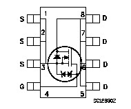
Features: ` WORLDWIDE LOWEST GATE CHARGE` TYPICAL RDS(on) = 0.11 ` HIGH dv/dt AND AVALANCHE CAPABILITIES` LOW INPUT CAPACITANCE` LOW GATE RESISTANCE` TIGHT PROCESS CONTROL AND HIGH MANUFACTORING YIELDSApplicationThe MDmesh™ family is very suitable for increasing power density allowing syste...
STSJ20NM20N: Features: ` WORLDWIDE LOWEST GATE CHARGE` TYPICAL RDS(on) = 0.11 ` HIGH dv/dt AND AVALANCHE CAPABILITIES` LOW INPUT CAPACITANCE` LOW GATE RESISTANCE` TIGHT PROCESS CONTROL AND HIGH MANUFACTORING YI...
SeekIC Buyer Protection PLUS - newly updated for 2013!
268 Transactions
All payment methods are secure and covered by SeekIC Buyer Protection PLUS.
The MDmesh™ family is very suitable for increasing power density allowing system miniaturization and higher efficiencies.

|
Symbol |
Parameter |
Value |
Unit |
|
VDS |
Drain-source Voltage (VGS = 0) |
200 |
V |
|
VDGR |
Drain-gate Voltage (RGS = 20 k) |
200 |
V |
|
VGS |
Gate- source Voltage |
±30 |
V |
|
ID
|
Drain Current (continuos) at TC = 25 Drain Current (continuos) at TC = 100 |
20
12.5 |
A
A |
|
IDM (2) |
Drain Current (pulsed) |
80 |
A |
|
Ptot Ptot |
Total Dissipation at TC = 25 Total Dissipation at TC = 25(1) |
70 3 |
W W |
|
dv/dt (3) |
Peak Diode Recovery voltage slope |
10 |
V/ns |
This 200V MOSFET STSJ20NM20N with a new advanced layout brings all unique advantages of MDmesh technology to lower voltages. The STSJ20NM20N exhibits worldwide lowest gate charge for any given on-resistance.Its use is therefore ideal as primary switch in isolated DC-DC converters for Telecom and Computer applications. Used in combination with secondary-side low-voltage STripFETTM products, it contributes to reducing losses and boosting efficiency.The exposed slug reduced the Rthj-c improving the current capability