THC63LVDF64A

Features: ·21:3 Data channel compression at up to·223 Megabytes per sec throughput·Wide Frequency Range: 20 - 85 MHz·suited for VGA,SVGA,XGA and SXGA·Narrow bus (8 lines) reduces cable size·345mV swing LVDS devices for Low EMI·Supports Spread Spectrum Clock Generator·On chip Input Jitter Filtering...

product image

THC63LVDF64A Picture
SeekIC No. : 004518651 Detail

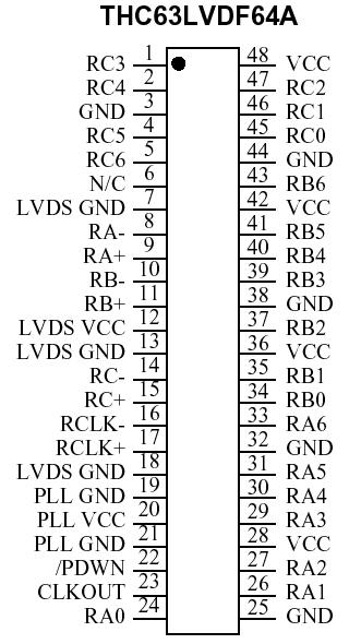
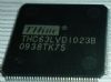
THC63LVDF64A: Features: ·21:3 Data channel compression at up to·223 Megabytes per sec throughput·Wide Frequency Range: 20 - 85 MHz·suited for VGA,SVGA,XGA and SXGA·Narrow bus (8 lines) reduces cable size·345mV sw...
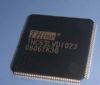
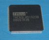
floor Price/Ceiling Price

Part Number:
THC63LVDF64A
Supply Ability:
5000

Price Break

  • Qty
  • 1~5000
  • Unit Price
  • Negotiable
  • Processing time
  • 15 Days
Total Cost: $ 0.00

SeekIC Buyer Protection PLUS - newly updated for 2013!

  • Escrow Protection.
  • Guaranteed refunds.
  • Secure payments.
  • Learn more >>

Month Sales

268 Transactions

Rating

evaluate  (4.8 stars)

Upload time: 2024/4/27

Payment Methods

All payment methods are secure and covered by SeekIC Buyer Protection PLUS.

Notice: When you place an order, your payment is made to SeekIC and not to your seller. SeekIC only pays the seller after confirming you have received your order. We will also never share your payment details with your seller.
Product Details

Description


Features:

·21:3 Data channel compression at up to
·223 Megabytes per sec throughput
·Wide Frequency Range: 20 - 85 MHz
·suited for VGA,SVGA,XGA and SXGA
·Narrow bus (8 lines) reduces cable size
·345mV swing LVDS devices for Low EMI
·Supports Spread Spectrum Clock Generator
·On chip Input Jitter Filtering
·PLL requires No External Components
·Single 3.3V supply with 110mW(TYP)
·Low Power CMOS Design
·Power-Down Mode
·Low profile 48 Lead TSSOP Package
·Clock Edge Programmable for Transmitter
·Improved Replacement for the National DS90CF363/364


Pinout

  Connection Diagram


Specifications

Supply Voltage (Vcc)  . . . . . . . . . . . . . . . . . . . . . . . . .  . . . . .-0.3 to +4V
CMOS/TTL Input Voltage  . . . . . . . . . . . . . .  . . .. . .-0.3V to (Vcc + 0.3V)
CMOS/TTL Output Voltage . . . . . . . . . . . . . . . . . . . -0.3V to (Vcc + 0.3V)
LVDS Receiver Input Voltage . . . . . . . . . . . . . . . . . -0.3V to (Vcc + 0.3V)
LVDS Driver Output Voltage . . . . . . . . . . . . . .. . . . -0.3V to (Vcc + 0.3V)
Output Short Circuit Duration continuous
Junction Temperature  . . . . . . . . . . . . . . . . . . . . . . . . . . . . . .  .+150°C
Storage Temperature Range . . . . . . . . . . . . . . .  . . . . -65°C to 150°C
Lead Temperature(Soldering, 4 sec.)  . . . . . . . . . . . . . . . . . . . .+260°C
Maximum Power Dissipation @25°C . . . . . . . . . . . . . . . . . . . . . . . 1.4W
Note 1:"Absolute Maximum Ratings" are those values beyond which the safety of the device cannot be guaranteed. They are not ment to imply that the device should be operated at these limits. The tables of "Electrical Characteristics" specify conditions for device operation.


Description

The THC63LVDM63A transmitter converts 21 bits of CMOS/TTL data into LVDS(Low Voltage Differential Signaling) data stream. A phase-locked transmit clock is transmitted in parallel with the data streams over a fourth LVDS link. The THC63LVDM63A can be programmed for rising edge or falling edge clocks through a dedicated pin.

The THC63LVDF64A receiver convert the LVDS data streams back into 21 bits of CMOS/TTL data with falling edge clock. At a transmit clock frequency of 85MHz, 18 bits of RGB data and 3 bits of LCD timing and control data (HSYNC, VSYNC, CNTL1) are transmitted at a rate of 595 Mbps per LVDS data channel.


Customers Who Bought This Item Also Bought

Margin,quality,low-cost products with low minimum orders. Secure your online payments with SeekIC Buyer Protection.
Circuit Protection
Static Control, ESD, Clean Room Products
Tapes, Adhesives
803
Connectors, Interconnects
Computers, Office - Components, Accessories
View more