
Tone Control
Index
Radio Advertising Voice Circuit
Published:2011/9/12 23:45:00 Author:Felicity | Keyword: Radio Advertising, Voice, Circuit
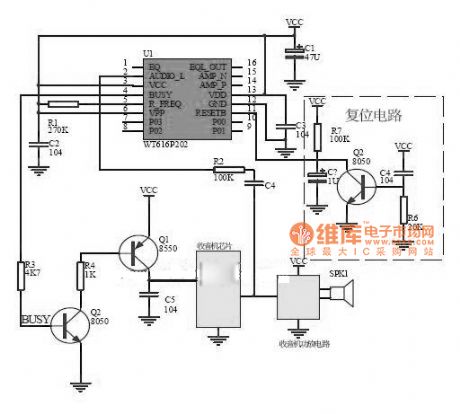
Work of the circuit
BUSY signal is the Uniquefeatureof the voice chip. We can use it to control the power circuit of the radio.
(View)
View full Circuit Diagram | Comments | Reading(1472)
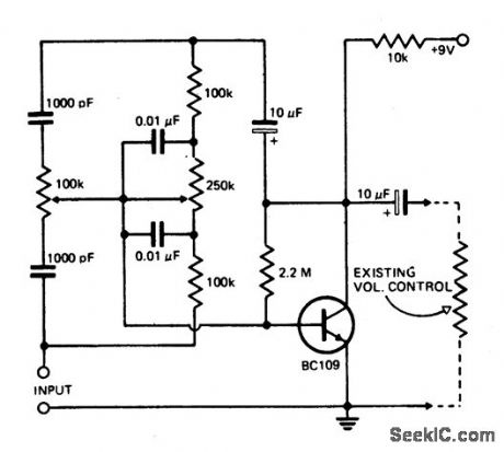
TONE_CONTROL_CIRCUIT
Published:2009/6/30 2:55:00 Author:May
A simple single-transistor circuit will give approximately 15 dB boost or cut at 100 Hz and 15 kHz respectively. A low noise audio type transistor is used, and the output can be fed directly into any existing amplifier volume con-trol to which the tone control is to be fitted. The gain of the circuit is near unity when con-trols are set in the flat position. (View)
View full Circuit Diagram | Comments | Reading(227)
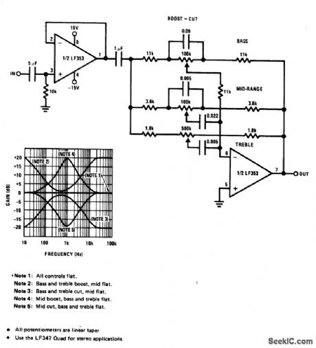
THREE_BAND_ACTIVE_TONE_CONTROL
Published:2009/6/30 2:49:00 Author:May
View full Circuit Diagram | Comments | Reading(0)
10_NOTE_SOUND_SYNTHESIZER
Published:2009/6/18 22:52:00 Author:May
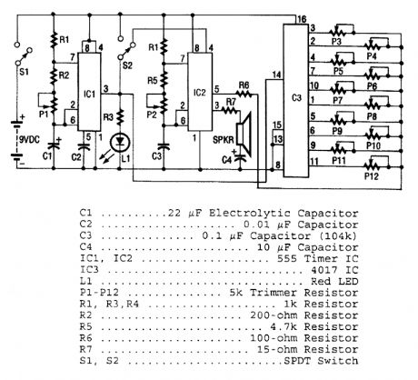
As shown, three ICs are used to produce the sounds. IC1 is a 555 timer that generates clock pulses. It is configured as an astable multivibrator. The frequency of the clock pulses is set by trim-mer potentiometer Pl. These clock pulses are coupled to the input of IC3 (a 4017 CMOS Johnson counter) on its clock input pin 14. Each clock pulse causes IC3 to shift a high to each of its output pins in sequence. A trimmer resistor, which can be adjusted to set a different frequency for each note, is connected to each of 103's output pins. One side of each of the trimmers is connected to pin 5 (the control voltage pin) of IC2.IC2, another 555 timer IC, creates the tone; the overall pitch of the tone can be varied by P2. As the output sequences from the 4017, that tone, which is changed in frequency by each output shift is applied to a srrtall speaker from pin 3 of IC2. An LED, which flashes with each clock pulse, is con-nected to pin 3 of IC1. Switch S2 is used to vary the sound between flowing and distinct notes. (View)
View full Circuit Diagram | Comments | Reading(1197)
TONE_CHIME
Published:2009/6/18 22:50:00 Author:May
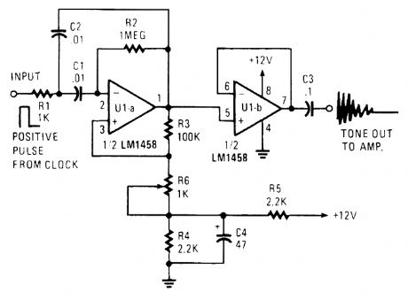
A positive pulse input to RI causes the active filter UI-a to ring. If the gain is set too high (R6), the circuit will oscillate. R6 controls the positive feedback and the Q of the circuit. C1 and C2 can be changed to adjust the tone frequency. (View)
View full Circuit Diagram | Comments | Reading(1135)
110_dB_BEEPER
Published:2009/6/18 22:45:00 Author:May
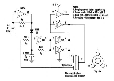
This circuit will gqnerate an ear-splitting 110 dB from 9 V. The setup uses a single 74C14 (CD40106B) CMOS hex inverting Schmitt-trigger IC, which must be used with a piezoelectric device with a feedback terminal. The feedback terminal is attached to a central region on the piezoelectric wafer. When the beeper is driven at resonance, the feedback signal peaks.One inverter of the 74C14 is wired as an astable oscillator. The frequency is chosen to be 5 times lower than the 3.2 kHz resonant frequency of the piezoelectric device. Feedback from the third pin of the beeper reinforces the correct drive frequency to ensure maximum sound output.Four other inverter sections of the IC are wired to form two separate drivers. The output of one section is cross-wired to the input of the second section. The differential drive signal that results produces about 18-V p-p when measured across the beeper. The last inverter section is wired as a second astable oscillator with a frequency of about 2 Hz. It gates the main oscillator on and off through a diode. For a continuous tone, the modulation circuit can be deleted. (View)
View full Circuit Diagram | Comments | Reading(1978)
Circuit Categories
power supply circuit
Amplifier Circuit
Basic Circuit
LED and Light Circuit
Sensor Circuit
Signal Processing
Electrical Equipment Circuit
Control Circuit
Remote Control Circuit
A/D-D/A Converter Circuit
Audio Circuit
Measuring and Test Circuit
Communication Circuit
Computer-Related Circuit
555 Circuit
Automotive Circuit
Repairing Circuit