
Tube Amplifier
Index
Typical application circuit diagram TDA2616 audio power amplifier circuit
Published:2014/1/13 18:35:00 Author: | Keyword: Typical application circuit diagram TDA2616 audio power amplifier circuit, TDA2616
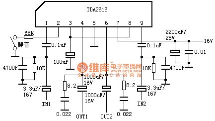
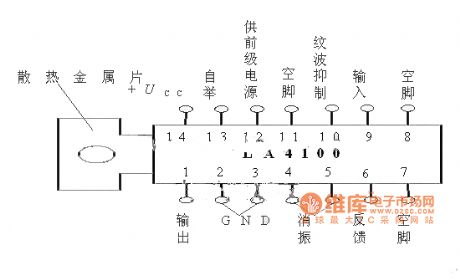
TDA2616 pin functions and reference voltage:
1 Foot: 10V - Signal Input 1
2 Feet: 5V - Squelch (low squelch)
3 Feet: 10V - 1/2 reference voltage
4 Feet: 10V - Signal output 1
5 feet: 0V - ground
6 Feet: 10V - Signal output 2
7 Feet: 20V - Power
8 feet: 10V - negative inputs
9 feet: 10V - Signal Input 2
Application Notes TDA2616 audio amplifier circuit shown in Figure typical
(View)
View full Circuit Diagram | Comments | Reading(11170)
NE5532 ore radio amplifier circuit diagram
Published:2014/1/13 18:30:00 Author: | Keyword: NE5532 ore radio amplifier circuit diagram, NE5532
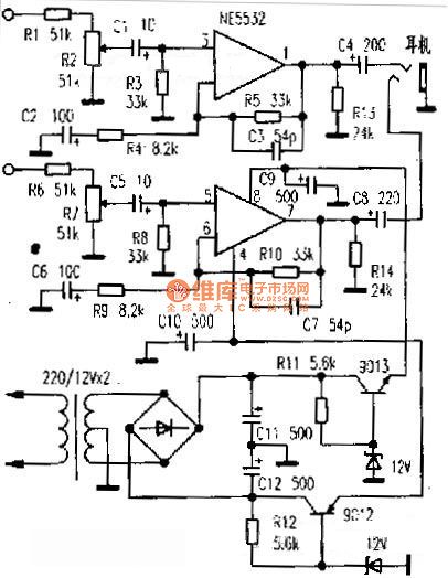
NE5532 ore radio amplifier circuit diagram as shown (View)
View full Circuit Diagram | Comments | Reading(2112)
Typical application circuit diagram TDA2009 audio power amplifier circuit
Published:2014/1/13 0:55:00 Author: | Keyword: Typical application circuit diagram TDA2009 audio power amplifier circuit, TDA2009
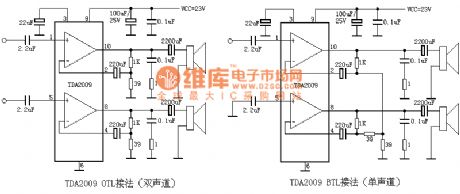
TDA2009
1-Foot: 1.2V-- Left channel input
2-Feet: 0.8V-- Left channel feedback
3 Feet: 12V - Squelch
4-Feet: 0.8V-- right channel feedback
5 Feet: 1.2V-- right channel input
6 Feet: 0V - ground
7 Feet: 0V - empty
8 feet: 12.4V-- right channel output
9 feet: 24V - Power
10 feet: 12.4V-- Left channel output
Application Notes TDA2009 audio amplifier circuit shown in Figure typical
(View)
View full Circuit Diagram | Comments | Reading(1971)
Typical application circuit diagram TDA1521 audio power amplifier circuit
Published:2014/1/13 0:38:00 Author: | Keyword: Typical application circuit diagram TDA1521 audio power amplifier circuit, TDA1521
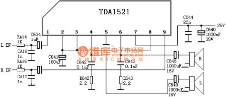
The circuit is taken from Changhong C2191, dual-channel access method for the OTL.
TDA1521 pin functions and reference voltage:
1 foot: 11V - Reverse Input 1 (L-channel signal input)
2 feet: 11V - Forward Input 13 feet: 11V - Reference 1 (when OCL connection to 0V, when OTL connection to 1/2Vcc)
4 feet: 11V - Output 1 (L-channel signal output)
5 feet: 0V - Negative power input (OTL connection when ground)
6 Foot: 11V - Output 2 (R channel signal output)
7 Foot: 22V - Positive power supply input
8 feet: 11V - positive input 2
9 feet: 11V - Reverse Input 2 (R-channel signal input)
Application Notes TDA1521 audio amplifier circuit shown in Figure typical
(View)
View full Circuit Diagram | Comments | Reading(3850)
Typical application circuit diagram TA8211AH audio power amplifier circuit
Published:2014/1/13 0:30:00 Author: | Keyword: Typical application circuit diagram TA8211AH audio power amplifier circuit, TA8211AH
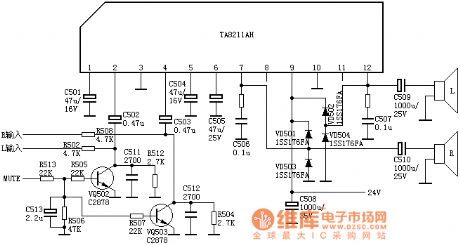
The circuit is taken from Changhong C2588-shaped TV
Pin 1: 2.1V-- Left channel negative feedback external capacitor
Pin 2: 2.2V-- left channel signal input
Pin 3: 0V - ground
Pin 4: 2.2V-- right channel signal input
Pin 5: 2.1V-- Right channel negative feedback external capacitor
Pin 6: 8.2V-- Power Filter
Pin 7: 12V - right channel signal output
Pin 8: 2.2V-- empty
Pin 9: 24V - Power
Pin 10: 2.2V-- empty
Pin 11: 12V - left channel signal output
Diagram TA8211AH typical audio amplifier circuit shown in Figure
(View)
View full Circuit Diagram | Comments | Reading(4699)
Typical application circuit diagram LA4287 audio power amplifier circuit
Published:2014/1/13 0:31:00 Author: | Keyword: Typical application circuit diagram LA4287 audio power amplifier circuit, LA4287
TV audio signal from ( 1 ) pin input N601 's , AV audio signal from ( 3 ) feet of the input N601 , CPU (40) pin output TV / AV switching signal via the base of R601 to V601 , V601 inverted by the after controlling N601 's ( 4 ) feet , after an internal selection ( 9 ) pin outputs an audio signal from the N601 , pushing the horn sound.
V641, V642 audio squelch circuit consisting shutdown : normal boot , 12V voltage is applied through R641 base V641 , V641 has been added to the emitter VD642 , VD642 because of the presence of so than the base -emitter voltage V641 high voltage 0.7V, V641 deadline , V642 also cut , this circuit has no effect on the volume control , then, the C641 is near the 12V charging voltage . After the shutdown , 12V voltage disappears , since the case is filled with the C641 12V voltage , so the base voltage V641 is lower than the emitter voltage , V641 conduction , V642 is also on, the volume control voltage is shorted to ground , to achieve a static off noise .LA4287 pin functions and reference voltage:
Pin 1 : 6.3V-- Signal Input 1
Pin 2 : 0V - ground
Pin3 6.3V-- Signal Input 2
Pin 4: 2.1V-- signal switch
Pin 5: 0.67V-- Volume control voltage input
Pin 6: 9.8V-- Filter
Pin 7: 9.8V-- Feedback
Pin 8: 0V - ground
Pin 9: 9.9V-- Output
Pin 10: 21V - Power
Diagram LA4287 typical audio amplifier circuit shown in Figure
(View)
View full Circuit Diagram | Comments | Reading(1691)
Typical application circuit diagram AN5265 audio power amplifier circuit
Published:2014/1/9 20:01:00 Author: | Keyword: Typical application circuit diagram AN5265 audio power amplifier circuit, AN5265
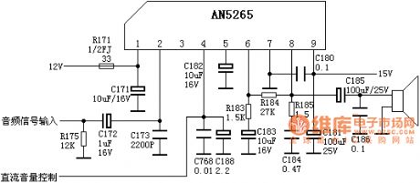
AN5265 pin functions and reference voltage:
Pin 1: 12V - Front-level power
Pin 2: 5V - audio signal input
Pin 3: 0V - Mute control terminal (high Mute)
Pin 4: 0.1V-- Volume control voltage input terminal
Pin 5: 7V - Filtering end
Pin 6: 7.4V-- Negative feedback input
Pin 7: 0V - ground
Pin 8: 7.5V-- the output of the power amplifier
Pin 9: 15V - power amplifier stage
Application Notes AN5265 typical audio amplifier circuit shown in Fig.
(View)
View full Circuit Diagram | Comments | Reading(4427)
Typical application circuit diagram LA4225A audio power amplifier circuit
Published:2014/1/9 19:58:00 Author: | Keyword: Typical application circuit diagram LA4225A audio power amplifier circuit, LA4225A
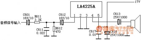
Diagram LA4225A typical audio amplifier circuit shown in Figure (View)
View full Circuit Diagram | Comments | Reading(1888)
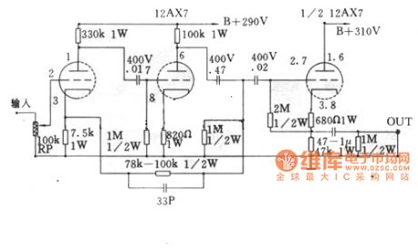
6 v6 bile machine circuit diagram
Published:2014/1/2 19:53:00 Author: | Keyword: 6 v6 bile machine circuit diagram,
Rectifier uses a buffer to protect the front 5Z4P level after level using two tubes using four 6P6P/6V6 use RiFa cathode capacitance, coupling capacitance adjustment silver foot audio tone.
6V6 tube amp circuit shown in Figure
(View)
View full Circuit Diagram | Comments | Reading(1659)
McLntosh C22 bile machine circuit diagram
Published:2014/1/1 19:43:00 Author: | Keyword: McLntosh C22 bile machine circuit diagram,
A circuit diagram as shown McLntosh C22 bile machine (View)
View full Circuit Diagram | Comments | Reading(1414)
Circuit Diagram of 2576+358+Voltage Regulator Tube Pattern
Published:2011/9/9 9:08:00 Author:Zoey | Keyword: Voltage Regulator Tube
Advantages:
(1) As 2576 has an interior overcurrent and overtemperature-proof device, it can input constant voltage, constant current CC and overvoltage proof OVP together with 358, so as to achieve a reliable, safe and perfect charge solution of lithium cells.
(2) EMI design of automobile charger is relatively easy for 2576 is a fixed 52-k PWM convertor.
(3)Both 2576 and lm358 are made in high pressure and dual polar, so they are very firm.
(4)This solution is usually used in automobile charger of 0.8A~1.5A.
Disadvantages:
(1) Its system is complex and costly.
(2) CC and OVP control the 2576 EN by 358’s input, therefore, the charge current has a relatively large wave, and corresponding speed of CC and OVP is not prompt enough.
(View)
View full Circuit Diagram | Comments | Reading(1271)
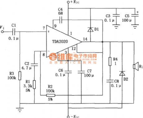
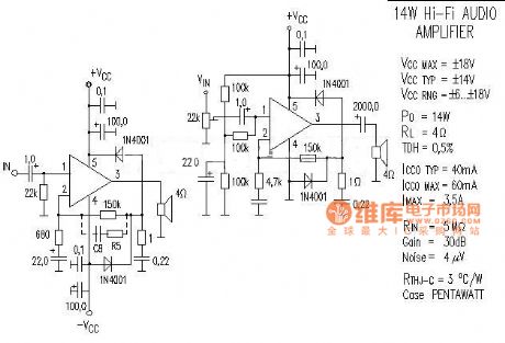
Typical application circuit diagram of 20W Hi—Fi audio power amplifier TDA2020
Published:2011/8/17 1:27:00 Author:Rebekka | Keyword: 20W Hi—Fi, Audio power amplifier , typical application
View full Circuit Diagram | Comments | Reading(3189)
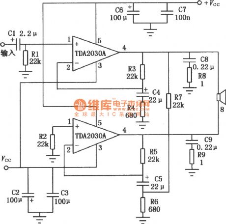
BTL application circuit diagram of TDA2030A audio power amplifier
Published:2011/8/17 2:25:00 Author:Rebekka | Keyword: Audio power amplifier , BTL application
View full Circuit Diagram | Comments | Reading(7071)
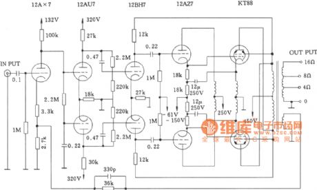
McIntosh Power Amplifier MC-275 Circuit
Published:2011/8/6 8:47:00 Author:Felicity | Keyword: McIntosh, Power Amplifier
View full Circuit Diagram | Comments | Reading(5757)
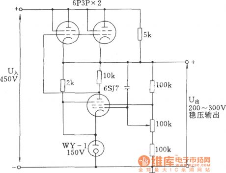
OTL Amplifier Power Current Circuit (For Tube Amp)
Published:2011/8/6 8:49:00 Author:Felicity | Keyword: OTL, Amplifier Power, Current Circuit, Tube Amp
View full Circuit Diagram | Comments | Reading(1917)
EL156 Tube Amp Circuit
Published:2011/8/6 8:52:00 Author:Felicity | Keyword: Tube Amp Circuit

View full Circuit Diagram | Comments | Reading(5556)
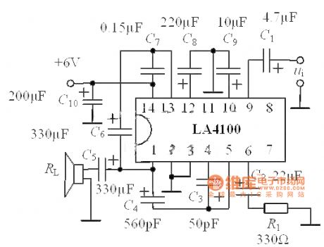
LA4100 Series Integrated Amplifier and Application Circuit
Published:2011/7/17 21:12:00 Author:Felicity | Keyword: LA4100 Series, Integrated, Amplifier, Application, Circuit
View full Circuit Diagram | Comments | Reading(4529)
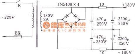
High-voltage Rectifier Circuit Of Side Thermal Rectifier Tube
Published:2011/7/17 20:56:00 Author:Felicity | Keyword: Side Thermal, Rectifier Tube, High-voltage Rectifier, Circuit
View full Circuit Diagram | Comments | Reading(1363)
Power Amplifier Circuit
Published:2011/7/17 21:01:00 Author:Felicity | Keyword: Power Amplifier, Circuit
View full Circuit Diagram | Comments | Reading(1382)
High-current Voltage Regulator Tube Circuit
Published:2011/7/17 21:08:00 Author:Felicity | Keyword: High-current, Voltage Regulator, Tube Circuit
View full Circuit Diagram | Comments | Reading(3156)
| Pages:1/2 12 |
Circuit Categories
power supply circuit
Amplifier Circuit
Basic Circuit
LED and Light Circuit
Sensor Circuit
Signal Processing
Electrical Equipment Circuit
Control Circuit
Remote Control Circuit
A/D-D/A Converter Circuit
Audio Circuit
Measuring and Test Circuit
Communication Circuit
Computer-Related Circuit
555 Circuit
Automotive Circuit
Repairing Circuit