
Index 125
Rectifier and filter circuit diagram
Published:2011/8/11 4:21:00 Author:nelly | Keyword: Rectifier, filter
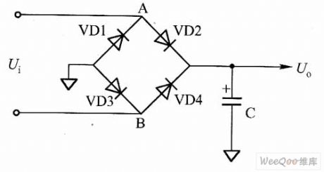
The function of the rectifier and filter circuit is to change AC into 300V DC voltage. The LCD power supply circuit often adopts bridge rectifier and capacitor filter type, the typical circuit is shown in the figure.
In the circuit, VD1~VD4 are four rectifier triodes of full bridge rectifier, C is filter capacitor, the capacity is large, the value of withstand voltage should be higher than 400V, Ui is the input AC voltage, Uo is the rectified outputed DC voltage, it always is about 300V.
(View)
View full Circuit Diagram | Comments | Reading(1269)
TEA1533 internal circuit diagram
Published:2011/8/11 5:40:00 Author:nelly | Keyword: internal circuit
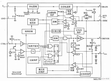
The adapted commercial power grid AC voltage range of switch power supply which is composed of TEA1533 is 70~276V, on the waiting state, the power consumption is lower than 3W.
TEA1533 has complete protection circuit, it includes: demagnetization protection, over-current protection, over-voltage protection, switch transformer winding short circuit protection, under-voltage protection, chip overheat protection and the safe soft-start circuit(decreasing output power) after the protection action, according to the commercial power grid rectified voltage, it can determine the IC's start voltage. TEA1533 also has the characteristics of soft-start .
(View)
View full Circuit Diagram | Comments | Reading(2199)
The VCO circuit diagram of dual D trigger
Published:2011/8/10 3:18:00 Author:nelly | Keyword: VCO, Dual D trigger
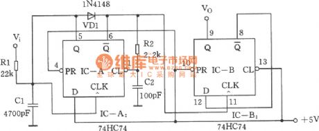
As shown in the figure, it is the VCO of dual D trigger. The circuit outputs a square wave signal with 50% duty cycle, the current consumption is low. When the input voltage is 5~12V, the output frequency range is 20~70KHz. Firstly, presuming IC-A's initial state is Q=low level. Then VD1 is cut off, C1 is charged by R1. When C1's voltage reaches the set level, IC-A is forced to reverse, the Q output terminal turns to high level, C1 is discharged by VD. At the same time, IC-A's CL input terminal turns to low level too, IC-A is forced to Q=low level.
(View)
View full Circuit Diagram | Comments | Reading(1049)
Pulse shaping circuit(CD4069)diagram composed of gate circuit
Published:2011/8/10 3:39:00 Author:nelly | Keyword: Pulse, shaping circuit, gate circuit
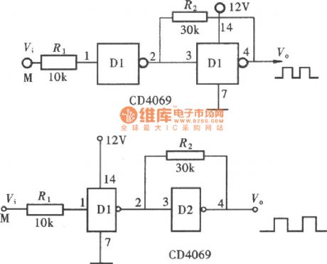
Due to the CMOS gate circuit has a fixed threshold level, for the part of signal pulse which is lower than threshold level, the gate circuit's input terminal is no answer. With this feature, it is often directly used for the pulse's shaping. In the electronic circuits, the integrated gate circuit is one of the common used circuits. Beside used as control gate, it is also used to form the clock pulse generator. An integrated gate circuit often contains several independent gate circuits, there are alway some spare parts after constituting the circuit's main structure.
(View)
View full Circuit Diagram | Comments | Reading(2127)
AP1510 typical application circuit diagram
Published:2011/8/11 5:08:00 Author:nelly | Keyword: typical application
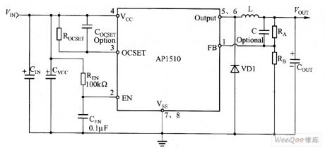
AP1510's 1 foot is the error feedback signal input terminal, 2 foot is output enabling terminal(high level enabling, when this foot is high level, 1 foot has output), 3 foot is oscillation set terminal(the maximum output current is set by the external resistance), 4 foot is voltage input terminal, 5, 6 feet are voltage output terminal, 7, 8 feet is groud connection. As shown in the figure, it is the AP1510 typical application circuit.
The working process of this circuit: under the control of the control circuit, the AP1510 internal switch tube is open. When the switch tube turns on, AP1510's 4 foot input voltage VIN is added to the internal switch tube S polar.
(View)
View full Circuit Diagram | Comments | Reading(984)
Voltage regulator DC-DC circuit and power supply monitor pins introduction and main features TA8001S constant voltage regulator
Published:2011/8/17 20:09:00 Author: | Keyword: Voltage regulator, power supply monitor, pins introduction, main features, constant voltage regulator
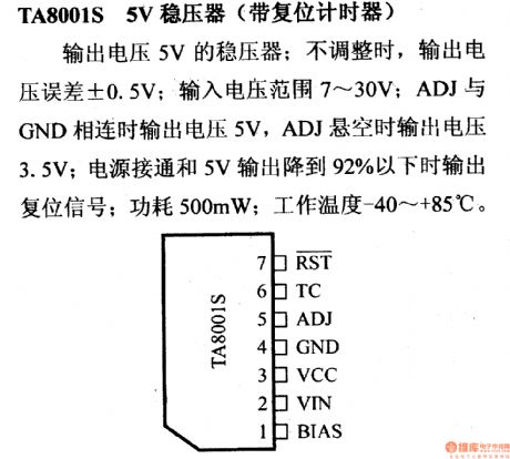
TA8001S constant voltage regulator
Its output voltage is 5 V with a difference of +/- 0.5 V. And its voltage coverage is from 7 V to 30 V. When ADJ is connected to GND, its output voltage is 5 V and when ADJ is suspended in midair, the output voltage is 3.5 V. It outputs restart signal when the power supply is connected and output voltage of 5 V lowers to 92% with the power consumption of 500mW. Its operating temperature is -40oC to +85oC. (View)
View full Circuit Diagram | Comments | Reading(870)
Voltage regulator DC-DC circuit and power supply monitor pins introduction and main features TA7900S constant voltage regulator
Published:2011/8/17 20:04:00 Author: | Keyword: Voltage regulator, power supply, main features
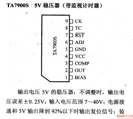
TA7900S constant voltage regulator
Its output voltage is 5 V with a difference of +/- 0.25 V. And its voltage coverage is from 7 V to 40 V. It outputs restart signal when the power supply is connected and output voltage of 5 V lowers to 92%. If the device makes mistake, the monitor will generate restart impulse with the power consumption of 500mW. Its operating temperature is -40oC to +85oC. (View)
View full Circuit Diagram | Comments | Reading(1438)
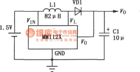
MM1126~MM1129 setting up DC-DC convertor
Published:2011/8/14 7:22:00 Author:leo | Keyword: DC-DC convertor, setting up
View full Circuit Diagram | Comments | Reading(693)
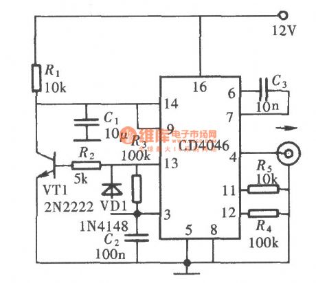
The scanning generator formed by CD4046
Published:2011/8/14 7:25:00 Author:leo | Keyword: Scanning, generator
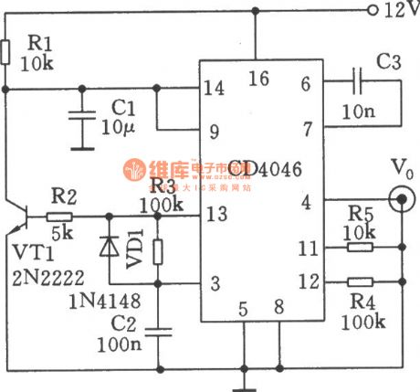
View full Circuit Diagram | Comments | Reading(1170)
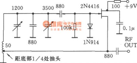
The imporved hartley circuit
Published:2011/8/17 20:23:00 Author: | Keyword: Hartley circuit
View full Circuit Diagram | Comments | Reading(711)
Voltage regulator DC-DC circuit and power supply monitor pins introduction and main features TA8505 power supply monitoring circuit
Published:2011/8/17 20:20:00 Author: | Keyword: Voltage regulator, power supply monitor, pins introduction and main features, power supply monitoring circuit
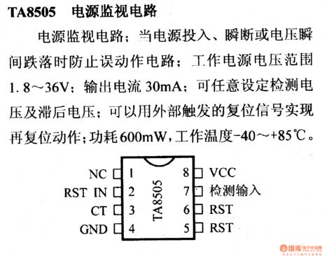
TA8505 power supply monitoring circuit When power supply is connected, cut off or voltage changes suddenly, the monitoring circuit will protect the circuit. Its operating voltage is from 1.8 V to 36 V with the output current of 30mA. It permits you set the test voltage or back-off voltage, which can use outer restart signal to carry out restart function. It has a power consumption of 600mW and the work temperature is from -40oC to +85oC. (View)
View full Circuit Diagram | Comments | Reading(985)
The frequency divider circuit with a rate of 34 and made by CD4017
Published:2011/8/14 7:14:00 Author:leo | Keyword: Frequency divider, rate
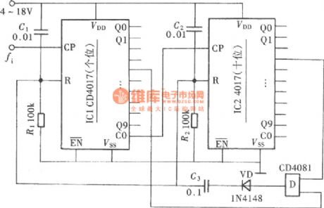
The frequency divider is formed by two CD4017 and dual input port. It can expand the frequency rate to 2 to 99 through different combinationsand connection, which is shown as following: (View)
View full Circuit Diagram | Comments | Reading(2686)
The frequency lock indicator formed by CD4046
Published:2011/8/14 7:17:00 Author:leo | Keyword: Frequency lock, indicator
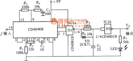
It can design a frequency lock indicator based the output features of two phase compatators of the lock circuit under the condition of locking frequency. (View)
View full Circuit Diagram | Comments | Reading(2778)
The sweeping signal generator formed by CD4046
Published:2011/8/14 7:27:00 Author:leo | Keyword: Sweeping signal, generator
View full Circuit Diagram | Comments | Reading(2994)
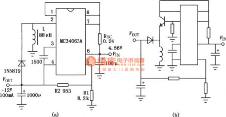
MC3406A reversible DC-DC convetor
Published:2011/8/11 11:15:00 Author:leo | Keyword: Reversible feature, DC-DC convetor
View full Circuit Diagram | Comments | Reading(1022)
Linear output integrated magnetic field sensor temperature compensation circuit
Published:2011/8/11 5:12:00 Author:John | Keyword: Linear output, integrated magnetic field sensor, temperature compensation
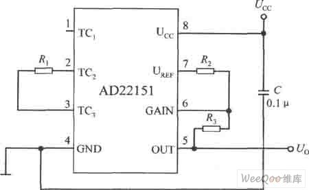
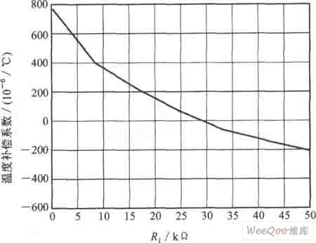
Constituted by the AD22151 bipolar mode temperature compensation circuit is as shown.
The circuit has the following characteristics: ① The temperature compensation resistor R1 is connected between the TC2 side and TC3 side; ② Zero magnetic field is biased on the UCC / 2; ③ It is able to compensate low temperature coefficient below the -500 × 10-6 / ℃. Under the bipolar mode, the curve between the resistance value of R1 and temperature compensation coefficient is shown. (View)
View full Circuit Diagram | Comments | Reading(1084)
Linear frequency output type humidity sensor and relative humidity measurement circuit
Published:2011/8/11 5:02:00 Author:John | Keyword: humidity sensor, relative humidity measurement
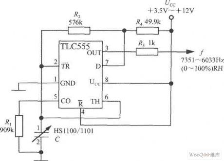
Linear frequency output type humidity sensor and relative humidity measurement circuit is as shown. The power supply voltage UCC ranges from +3.5V to +12 V. Utilizing a CMOS timer TLC555, HS1100/1101 and resistors R2 and R4 are coupled to constitute a monostable circuit. Then the relative humidity is converted into frequency signal. The output frequency ranges from 7351 Hz to 6033Hz and its corresponding relative humidity is from 0 to 100%. When RH = 55%, f equals to 6660Hz. Output frequency signals can be sent to the digital frequency meter or SCM system for measuring and displaying the relative humidity values. R3 is the current limiting resistor of the output end, ensuring the protective effect.
(View)
View full Circuit Diagram | Comments | Reading(2768)
Automatic cycle timer circuit diagram
Published:2011/8/11 2:42:00 Author:Rebekka | Keyword: Automatic cycle timer
Automatic cycle timer circuit diagram is shown as above. It is composed of pulse oscillator, time base circuit composed of multi-level divider, double-contact state trigger, the relay, driver circuit and the power supply etc. (View)
View full Circuit Diagram | Comments | Reading(1703)
Precision adjustable timer(CD4017) circuit diagram
Published:2011/8/11 2:39:00 Author:Rebekka | Keyword: Precision adjustable timer
Precision adjustable timer(CD4017) circuit diagram is shown as above.
It uses crystal oscillator composed of CD4060 and quartz crystal to generate base signal. It is an adjustable timer using multi-level digital frequency circuit to make frequency division. (View)
View full Circuit Diagram | Comments | Reading(2582)
Any input voltage converting into 4 ~ 20mA V/ I converter circuit diagram
Published:2011/8/16 21:39:00 Author:Rebekka | Keyword: V/ I converter circuit , 4 ~ 20mA
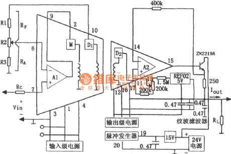
Any input voltage converting into 4 ~ 20mA V I converter circuit composed of isolated amplifier 3656 is shown as above.3656 amplifier is an isolated amplifier whichuses a hybrid integrated circuit for signal amplifier and isolation of power supply. It has a strong processing ability of analog signal because it uses an advanced modulation techniques and small hybrid transformer. The outstanding advantages of 3656 are: High adaptability and excellent performance. The ground terminals of input circuit, output circuit and power circuit are independentto each other. And they are not connected with each other to achieve the three-port isolation. (View)
View full Circuit Diagram | Comments | Reading(989)
| Pages:125/471 At 20121122123124125126127128129130131132133134135136137138139140Under 20 |
Circuit Categories
power supply circuit
Amplifier Circuit
Basic Circuit
LED and Light Circuit
Sensor Circuit
Signal Processing
Electrical Equipment Circuit
Control Circuit
Remote Control Circuit
A/D-D/A Converter Circuit
Audio Circuit
Measuring and Test Circuit
Communication Circuit
Computer-Related Circuit
555 Circuit
Automotive Circuit
Repairing Circuit