
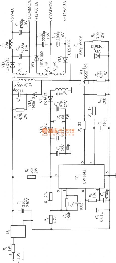
Index 90
DZW75-48/5050II power factor compensation
Published:2011/12/4 20:50:00 Author:May | Keyword: power factor compensation
The elementary diagram of DZW75-48/5050II power factor compensation:
DZW75-48/5050II power factor compensation circuit:
In the diagram, (a) is compensation circuit, (b) is auxiliary power supply. It mainly consists of N1, power factor calibration control module and some support circuits. N1 internal circuit consists of saw-tooth wave generator, pulse width modulator and multiple comparator circuit and so on. The frequency of saw-tooth wave generator is determined by out-connected capacitor and resistor. This machine makes the frequency of its output pulse work at 50 kHz, and the width of output pulse is determined by the error voltage after a general comparison treatment. It has three sampling and comparison circuits. V6 is actually an integrated chip containing VMOS tube,enhance diode and rectifier bridge. (View)
View full Circuit Diagram | Comments | Reading(940)
DZW75-48/5050II high frequency converting circuit
Published:2011/12/4 20:29:00 Author:May | Keyword: high frequency converting
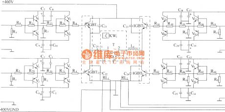
High frequency converter adopts full bridge structure. IGBT in four arms are separately driven by four drivers which are mutual isolated. Their working power supply is 300V. Under the effect of drive pulse, high frequency switching tubes on the two crosses are turned on at the same time, or cut off at the same time, thereby getting high frequency pulse voltage at main transformer’s first and second coils, in order to achieve high frequency conversion of DC/AC. When both 1# and 4# drive pulses are in positive potential, IGBT1, IGBT4 are turned on at the same time, at this time, both the drive pulse of IGBT2 and IGBT3 are in negative potential, cut off reliably, the first coil of main transformer T will have current, the current direction is from 1 end to 2 end, and the primary induced voltage is set to positive pulse, and its width is about 300V. (View)
View full Circuit Diagram | Comments | Reading(718)
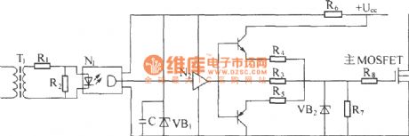
DZW75-48/5050II steady voltage and current limiting, current sharing circuit
Published:2011/12/4 20:22:00 Author:May | Keyword: steady voltage, current limiting, current sharing
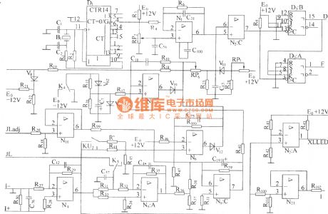
The steady of output voltage is mainly using the principle of negative feedback, the sample value of output value is returned back to error comparator, and it uses error voltage output by error comparator to control or modulate (adjust) the output pulse width of pulse width modulator, thereby adjust the height of output voltage to achieve the purpose of steady voltage output. As shown in the diagram, sampling voltage LOAD (-) is sent to “-” end of error comparator N3 resistor R19, then the “+” end of N3 is connected to -4.3V reference voltage offered by -12V power supply and voltage regulator diode V9 by resistor R17, when it is in normal operation, K4 contact point lies to -12V. In fact, N3 is a different amplifier.
(View)
View full Circuit Diagram | Comments | Reading(809)
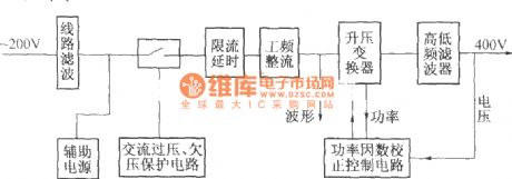
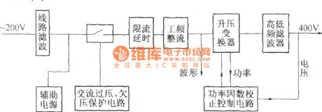
DZW75-48/5050II input circuit
Published:2011/4/14 6:11:00 Author:may | Keyword: input
(1) 220V (5Hz) alternating voltagepass Z1 circuit filter filtering, then it will send to the connect point of AC over voltage, under voltage protect relay K2. When normal working, K2 connect point should up-close, connect AC 220V voltage to AC current-limiting resistance R4 (after starting up, delay period of time, R1 is short-circuit by K1 connect point), send to power frequency bridge rectifier rectifying, get DC 300V output voltage through parallel connection condenser bank smoothed filtering, finish power frequency AC/DV transform. R2 is leak resistance.
(2) Z1 circuit filter is used for suppressing and absorbing obstruction of strong pulse to rectifier on electric network, increasing the reliability of rectifier. At the same time, the good common mode and difference module insertion loss of circuit filter can effectively inhibit inverted output high frequency interfering signal generated by high frequency switching converter,it canisolate rectifier and electric fence, avoid mutual interference.
(3) AC over voltage, under voltage protection circuit, AC 220V voltage sended to reducing transformer after through circuit filter filtering.
(4)AC current limiting delay circuit, AC voltage can switch-in machine in normal work range, build time at auxiliary power supply after AC power supply switch-in, andby a period of time delay after auxiliary power supply build, it can make AC current-limiting resistance short-circuit, this period time is AC current limiting delay, it is finish by AC current limiting delay circuit. (View)
View full Circuit Diagram | Comments | Reading(1472)
Introduction of high frequency winding coiling
Published:2011/11/23 2:27:00 Author:May | Keyword: high frequency winding, coiling
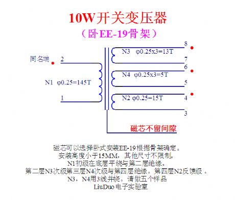
Introduction of high frequency winding coiling (switching power supply 12W transformer dual group with feedback group)
10W switching power transformer
Magnetic core can choose horizontal type installing EE-19 and determined by skeleton.
Installing height is less than 15mm. Other sizes have no limit.
N1 primary coil is row winding at bottom level and is isolated from second level.
Second level N3, secondary level, third level, N4 levelare isolated with fourth level. Fourth level N2 isin feedback level.
N3, N4are using three wires to winding together. (View)
View full Circuit Diagram | Comments | Reading(1369)
The special chip driving high-fidelity and pure sine wave inverter 1 based on Class D amplifier
Published:2011/11/10 2:18:00 Author:May | Keyword: Class D amplifier, special chip, sine wave inverter
View full Circuit Diagram | Comments | Reading(6720)
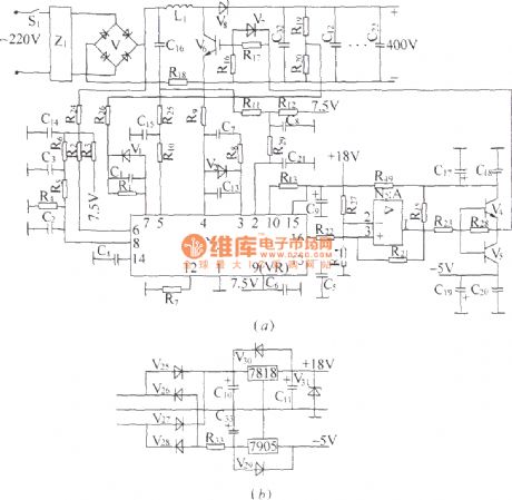
DZW75-48/50(50II) type power factor compensation
Published:2011/12/5 1:13:00 Author:May | Keyword: power factor compensation
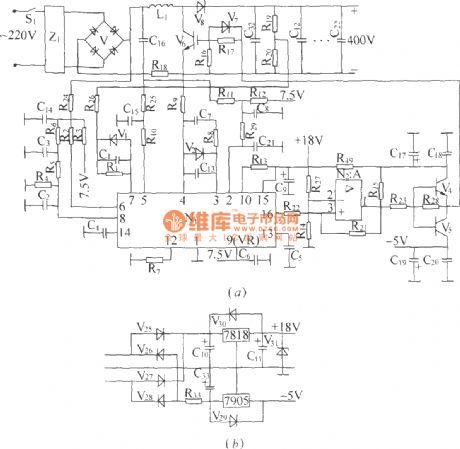
The elementary diagram of DZW75-48/5050II power factor compensation:
DZW75-48/5050II power factor compensation circuit:
In the diagram, (a) is compensation circuit, (b) is auxiliary power supply. It mainly consists of N1, power factor calibration control module and some support circuits. The internal part of N1 consists of saw-tooth wave generator, pulse width modulator and multiple comparator circuit and so on. The frequency of saw-tooth wave generator is determined by out-connected capacitor and resistor. This machine make the frequency of its output pulse work at 50 kHz, and the width of output pulse is determined by the error voltage after a general comparison treatment. It has three sampling and comparison circuits. In fact, V6 is integrated chip consisting VMOS tube, promotion diode and rectifier bridge.
(View)
View full Circuit Diagram | Comments | Reading(689)
DZW75-48/50(50II) high frequency rectifying filtering circuit
Published:2011/11/23 1:27:00 Author:May | Keyword: high frequency rectifying, filtering
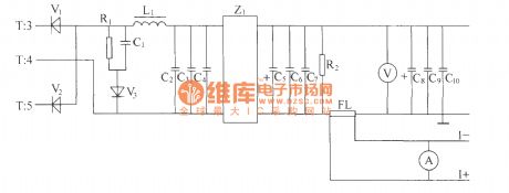
Positive and negative alternation pulse voltage of high frequency transformer T’s secondary induction pass full wave rectifier composed of high frequency switching diodes V1, V2, then pass L power line filter composed of L1 inductor and capacitor C2, C3, C4 and Z 1 :power supply filter and other smoothing filters,then the output end gets 48V DC voltage output with high and low frequency noise to meet the index demand. The pulse width isdirectly decided bythe output voltage. When the pulse width is wide, the output voltage will be high; if the pulse width is narrow, output voltage islow. In order to measureanddisplay output DC voltage, we can parallel connect a voltmeter in output end. R2 is the leak resistor. FL is thecurrent divider. The voltage value in the justify of FL also can be uses as output current sampling signal and itcan besent to stabilize voltage and limit current. R1, C1 and V3 make up the RCD absorber circuit to absorb overshoot voltage of secondary. (View)
View full Circuit Diagram | Comments | Reading(587)
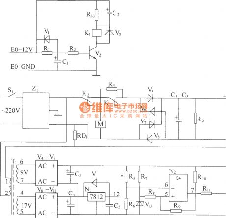
The driver circuit of switching power supply
Published:2011/12/4 21:35:00 Author:May | Keyword: driver, switching power supply
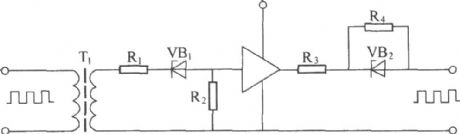
Driver circuit principle diagram:
Driver circuit of switching power supply:
The main function of driver circuit is enlarge the variable width pulse output by pulse width controller forthe driver signal of high voltage power supply switching device. Driver circuit generally has theisolatingfunction. It always uses transformer coupling mode to energizethe high voltage power switching device and isolate input stage and output stage. Meanwhile it can add reverse bias when power switching device is cut off to increase the speed of cut-off device. When it drives MOSFET devices, the common driver circuit is achieved by a driver transformer. (View)
View full Circuit Diagram | Comments | Reading(859)
5V/10A 100kh choking transducer XDUCER using SIPMOS transistor
Published:2011/11/22 1:42:00 Author:May | Keyword: 5V/10A, 100kh , choking transducer XDUCER , SIPMOS transistor
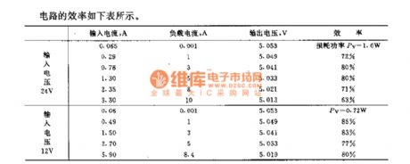
This circuit can convert 24V DC voltage to output DC voltage with low voltage. Its switching transistor uses SIPMOS tube BUZ23, andits featuresare thatlimiting frequency is much higher and needed controlling power is very small. In order to have higher switching frequency, the circuit adopts thechoke with small inductance value and filter capacitors C1~C3 with small capacitance.
The efficiency of this circuit is shown in the following table.
(View)
View full Circuit Diagram | Comments | Reading(962)
5V/10A 20kHz blocking communication device using SIPMOS transistor
Published:2011/11/23 1:54:00 Author:May | Keyword: 5V/10A 20kHz, blocking communication device, SIPMOS transistor
This circuit is convertor which can change input DC voltage (+20~+30V) to lower DC output voltage (+5V). Integrated circuit TDB0555B is time base circuit which can generate 20kHz square wave. The timing time of output (pin 3) is between 10~40μs. Fixed bias can make T1 to break over. Square wave voltage output by TDB0555B is differential to triangle wave voltage by R4, C5 and R6+R7. It also can make T1 cut off. So T1's output is square wave. Then the transformer can output AC and DC voltage after rectifying and filtering before passing opposite phase grade, drive grade and power amplifier grade.Main technical data: input voltage: +20~30V (rated value is 24V);output voltage: +5V;output current: 10A;network voltage adjustment rate: ±0.5%;load voltage adjustment rate: ±2%;efficiency: 78% (when the input voltage is 24V) (View)
View full Circuit Diagram | Comments | Reading(591)
Zero type recitfying and stabilizing voltage circuit
Published:2011/11/23 2:06:00 Author:May | Keyword: Zero type, recitfying, stabilizing voltage
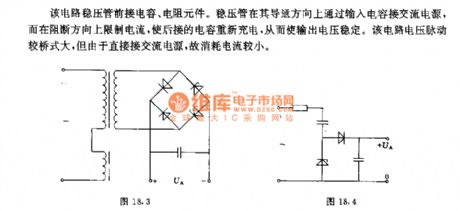
In this circuit, it connects to thecapacitor and resistor components in front of voltage regulator tube. Voltage regulator tube connectsto AC power supply by input capacitor in the direction of breaking over, but it limits current in the direction of breaking. It can make the followed capacitor recharge. Thereby it can make the output voltage be stable. Voltage pulse of this circuit is larger than bridge type circuit. Because it is directly connected with AC power supply, its consumption current is small. (View)
View full Circuit Diagram | Comments | Reading(612)
The special chip driving high-fidelity and pure sine wave inverter based on Class D amplifier
Published:2011/11/10 2:18:00 Author:May | Keyword: Class D amplifier, specialchip sine wave inverter

View full Circuit Diagram | Comments | Reading(6692)
DC voltage converter with output voltage U>100V and phase power Po=25W
Published:2011/12/5 1:17:00 Author:May | Keyword: DC voltage converter, output voltage U>100V, phase power Po=25W
This circuit works by the principle of blocking converter. That is, it can send energy to load in the period when transistor is cutting off. Divider circuit R1, R2 and C2are used for guarantee the circuit can start reliable oscillation when input voltage Ui≥2V. The circuits can non-load operate in a short time. But it does not have the function of protection when output end is short.
The main technical data of this circuit:
Output power: Po=2.5W;
Output voltage: Uo≥100V;
Oscillation frequency: f≈20kHz;
Efficiency: η=0.76.
Transistor data:
n1=50turns, 0.33 copper enamel wire;
n2=13turns, 0.1mm copper enamel wire;
n3=50turns, 0.3mm copper enamel wire. (View)
View full Circuit Diagram | Comments | Reading(530)
一1.5V-120V/10MV DC voltage converter
Published:2011/12/5 1:15:00 Author:May | Keyword: 一1.5V-120V/10MV, DC, voltage converter
It best adopts single end blocking converter to change 1.5V voltage into 120V voltage. The reason is that the voltage changing at this time is higher than transformer's. Its working process: transformer stores energy in the period when the transistor is breaking over, but it will send the energy to load in the period when it is cutting off.
Main technical data:
Working voltage: 1.5V;
Working current: 16mA;
Output voltage: 120V;
Load resistance: 1MΩ;
Frequency: 5kHz.
Transformer data:
n1=100turns, 0.12mm copper enamel wire;
n2=50turns, 0.05mm copper enamel wire;
n3=1000turns, 0.05 copper enamel wire. (View)
View full Circuit Diagram | Comments | Reading(1362)
The single-ended reflection converter circuit composed of CW1842 and external connected MOS power transistor
Published:2011/11/22 1:36:00 Author:May | Keyword: single-ended, reflection converter , external connected, MOS power transistor
View full Circuit Diagram | Comments | Reading(690)
The resonant converter schematic diagram based on step-down circuit (series)
Published:2011/11/22 1:09:00 Author:May | Keyword: resonant converter , step-down circuit
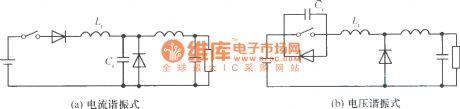
In the generalused switching stabilized voltage supply, it can use theresonantswitch to replace the step-down convertor's shape, and that is the resonant converter circuit. The diagram shows the example of changing step-down convertor to resonant converter: diagram (a) is current resonant ; diagram (b) is voltage resonant.
(View)
View full Circuit Diagram | Comments | Reading(1359)
Full bridge power inversion circuit
Published:2011/11/14 2:35:00 Author:May | Keyword: Full bridge, power inversion
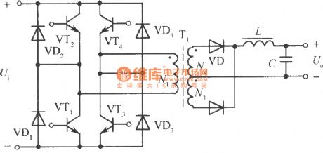
Full bridge inversion circuit is shown in the diagram and consists of suitable driver circuit and half bridge converter which hastwo electrolytic capacitors. Four bridge arms consist of VT1, VT2, VT3 and VT4. High frequency transformer T is connected in the middle of them. VT1, VT4 and VT2, VT3 on opposite arms is breaking over in turns by excitation of drive circuit. They can change DC input voltage to high frequency square wave AC voltage. Its working process is the same as push pull power converting circuit. So when high frequency transformer is working, the voltage gotten by its primary coil is power supply voltage. It is one time of half bridge circuit's output voltage, but each transistor's withstand voltage is still power supply voltage, so the output voltage is enlarging one time. If you want to let the current reach the level of half bridge circuit, the current shoule be enlarged one time, the output power can beenlarged four times.
The main shortcoming of full bridge circuit is that it needs four groups transistors base drive circuit which are isolatingfrom each other, so the control drive circuit is complex and expensive. (View)
View full Circuit Diagram | Comments | Reading(1054)
4~20mA current transmitter circuit with digital pressure signal disposal device MAX1459
Published:2011/8/31 1:47:00 Author:Jessie | Keyword: current transmitter, digital pressure signal disposal device
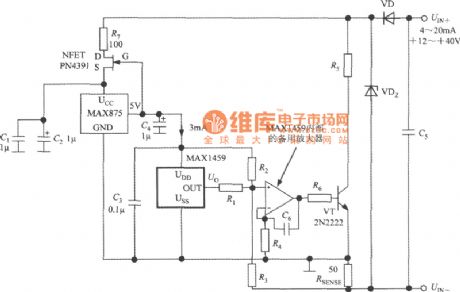
PGA's output voltage is sentto spare amplifier in chip, then we can get 4~20mA output current by external power amplifier circuit. In long-distance transmission current, the current signal's precision is not influenced by the resistance of cable. PN4391 is a 40V, 150mANFET. MAX875's voltage temperature coefficient is 7×10⁻⁶/℃. The 3mA constant current source iscomposedof PN4391 and MAX875, and it provides stable work current to MAX145, then it uses MAX1459 to take temperature compensation and gain compensation. MAX1459's output voltage is converted into 4 ~ 20mA current signal through backup amplifier and power amplifier, and its loop power range is + 12 ~ 40V. VT uses 2N2222 power tube, and its main parameters are: UCEO = 60 V, ICM = 0.8 A. The initial voltage of measuring resistance is set by resistors R1 ~ R 4, and the signal voltage of RSENSE is controlled by MAX1459. (View)
View full Circuit Diagram | Comments | Reading(2291)
Temperature measurement instrument circuit with thermocouple cold end temperature compensator AD596/597
Published:2011/8/30 21:45:00 Author:Jessie | Keyword: Temperature measurement instrument, thermocouple cold end temperature compensator
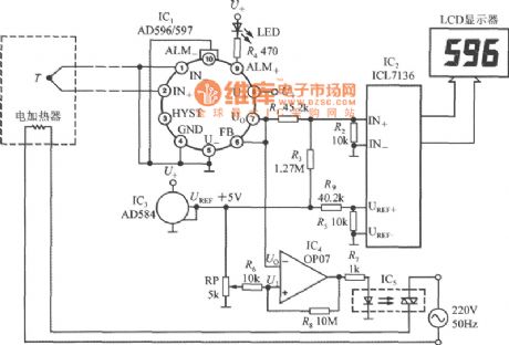
AD596/597 is used as a closed-loop thermocouple signal disposal implement. IC2 is CMOS monolithic 3 1/2 A/D converter ICL7136,which can be replaced byusing ICL7106, but power consumption will increase a little. IC3 is +5V bandgap benchmark voltage source AD584, +5V benchmark voltage provides1.000V benchmark voltage to ICL7136 after separated voltage by R4, R5, DPMwith full range in 2V is composedof ICL7136 and LCD display. IC4 chooses OP07 operational amplifier. RPis a setting point adjust potentiometer, which is used to set the controlling temperature T1. IC5 is TRIAC's optical coupler. (View)
View full Circuit Diagram | Comments | Reading(2339)
| Pages:90/471 At 2081828384858687888990919293949596979899100Under 20 |
Circuit Categories
power supply circuit
Amplifier Circuit
Basic Circuit
LED and Light Circuit
Sensor Circuit
Signal Processing
Electrical Equipment Circuit
Control Circuit
Remote Control Circuit
A/D-D/A Converter Circuit
Audio Circuit
Measuring and Test Circuit
Communication Circuit
Computer-Related Circuit
555 Circuit
Automotive Circuit
Repairing Circuit