
Index 87
The measuring infinitesimal displacement with optical emission components
Published:2012/8/15 22:49:00 Author:Ecco | Keyword: measuring , infinitesimal displacement , optical emission components
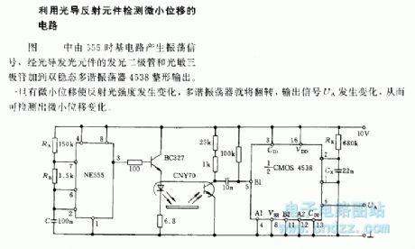
The 555 time-base circuit in the figure can generate oscillation signal, and it is added to the bistable multi -vibrator 4538 by photoconductive light-emitting diode and phototransistor, then it is shaped and output. Once there is a slight displacement makes the reflected light intensity change, the multivibrator will flip, then output signal UA changes, therefore the small displacement can be detected.
(View)
View full Circuit Diagram | Comments | Reading(1018)
The line mode acousto-optic voltmeter circuit with variable range of 1.2 to 1000V
Published:2012/8/15 22:53:00 Author:Ecco | Keyword: line mode , acousto-optic voltmeter , variable range , 1.2 to 1000V
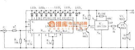
As shown in the figure, it is composed of the LED driver circuit, voice circuit, audio amplifier circuit, and it uses 10 LEDs to display linear voltage between 1.2 ~ 1000V, when the voltage is closed to the upper limit voltage, the circuit will issue a protected voice signal.
(View)
View full Circuit Diagram | Comments | Reading(1065)
The structure schematic of antimonide indium Hall elements
Published:2012/8/16 22:32:00 Author:Ecco | Keyword: structure schematic, antimonide indium, Hall elements
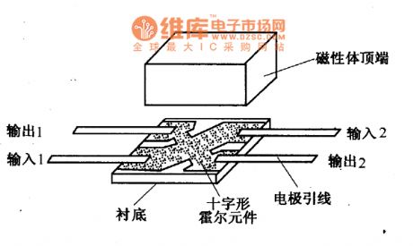
The figure shows the structure of antimonide indium Hall elements made by a sputtering process, and it consists of substrate, cross-shaped Hall element, electrode lead and the top of the magnetic body. In the leads of cross Hall element's four ends, one pair are current input ends, the other are the Hall voltage output ends. The top of the magnetic body is set in order to concentrate the magnetic field lines and the element sensitivity, and its volume of components is larger, the output sensitivity is higher.
(View)
View full Circuit Diagram | Comments | Reading(765)
TV small-signal processing monolithic integrated circuit diagram
Published:2012/8/16 21:41:00 Author:Ecco | Keyword: TV , small-signal processing, monolithic, integrated circuit
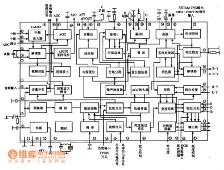
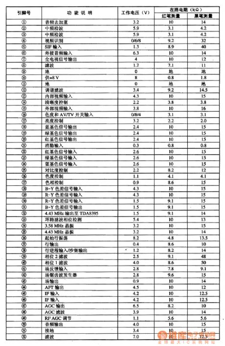
DA8362 is the TV small-signal processing monolithic integrated circuit produced by Philips, which are widely used in a variety of import- brand and domestic large-screen color TVs.(1) Features and functionsTDA8362 IC includes image and audio signal processing circuit, line and field scanning signal processing circuit, chrominance and luminance signal processing circui, character display signal processing circuit, external video or luminance (Y) signal input circuit, sync separator and some other circuits with auxiliary functions. Its internal block diagram is shown in Figure 1.(2) pin functions and dataThe TDA8362 IC uses 52-pin dual in-line package, and pin functions and data are listed in Table 1.
(View)
View full Circuit Diagram | Comments | Reading(1756)
ST6368B4-FHO single-chip microcomputer integrated circuit diagram
Published:2012/8/16 20:14:00 Author:Ecco | Keyword: single-chip , microcomputer, integrated circuit
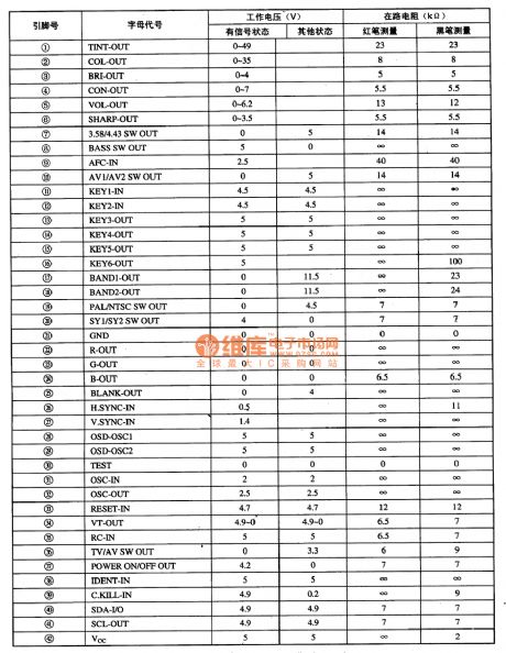
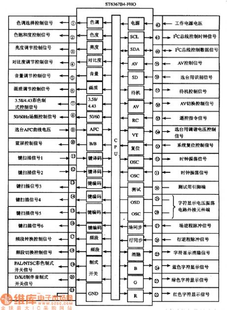
ST6368B4-FHO is a single - chip microcomputer IC which is widely used in Konka series of large-screen digital color TVs.(1) FeaturesST6368B4-FHO IC integrates central processing unit (CPU), clock oscillation circuit, reset circuit, key scan pulse generating circuit, key scan command signal decoding circuit, I2C bus control circuit, screen display circuit, system control circuit, remote control instruction signal processing circuit and other control circuits and other components with additional functions.(2) pin functions and dataST6368B4-FHO IC uses 42 - pin dual in-line package, and the internal block diagram, pin functions and signal flowing are shown as the chart, and pin-letter code and data are shown in following Table.
(View)
View full Circuit Diagram | Comments | Reading(1236)
STK6722H motor control and driver IC diagram
Published:2012/8/16 20:21:00 Author:Ecco | Keyword: motor control , driver IC
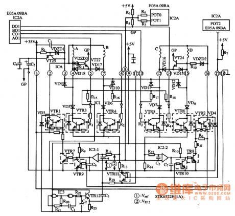
STK6722H is the thick-film hybrid motor control and drive IC produced by Japan Sanyo, and it is widely used in the printer.
(1) pin functionsSTK6722H IC uses 18 - pin separate package, and pin functions are shown in following Table .
(2) Typical application circuitSTK6722H integrated circuit's internal circuit and the application circuit of printer control and driver circuit are shown in the figure.
(View)
View full Circuit Diagram | Comments | Reading(2255)
STR - F6653 switching power thick-film integrated circuit diagram
Published:2012/8/16 20:30:00 Author:Ecco | Keyword: switching power, thick-film , integrated circuit

STR - F6653 is the switching power thick-film integrated circuit produced by Japan Sanyo, and it is widely used in Toshiba series of large-screen digital color TVs.
(1) Features and functionsSTR-F6653 IC contains incentives driver control circuit, start circuit, oscillation circuit, overcurrent protection circuit, overvoltage and overtemperature protection circuit and other ancillary unit circuits.
(2) pin functions and dataSTR - F6653 uses a separate pin package, and the pin functions and data are shown in following Table.
(3) Typical application circuitSTR - F6653 IC consisting of a typical application circuit of the switching power supply circuit as shown.
(View)
View full Circuit Diagram | Comments | Reading(8295)
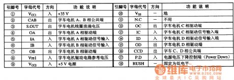
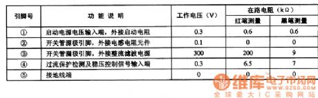
STR - D6802 switch power thick-film integrated circuit diagram
Published:2012/8/16 20:26:00 Author:Ecco | Keyword: switch , power , thick-film , integrated circuit
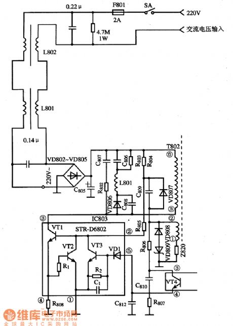
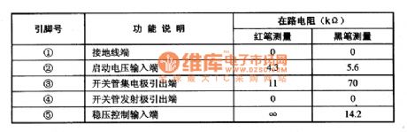
STR-D6802 is the switching power thick-film integrated circuit produced by Japan Sanyo, and it is widely used in large screen color TV and DVD player.(1) Features and functionsSTR-D6802 IC contains the start, oscillation, driver, overcurrent protection circuits.(2) pin functions and dataSTR-D6802 uses a separate pin package, and the pin functions and data are shown in following Table .(3) Typical application circuit
(View)
View full Circuit Diagram | Comments | Reading(1985)
STR-F6656B, STR-F6658B switching power thick-film integrated circuit diagram
Published:2012/8/16 20:45:00 Author:Ecco | Keyword: switching power, thick-film , integrated circuit
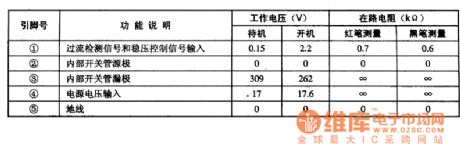
STR-F6656B, STR-F6658B are the swicthing power hybrid thick-film integrated circuits produced by Sanken, and they are widely used in large screen color TVs and DVD players.
(1) Features and functionsSTR-F6656B and STR-F6658B have the basically same internal functions( the following is an example of STR-F6658B), both of them are composed of start circuit, oscillation circuit, driver circuit, overcurrent protection circuit, overvoltage protection circuit and overheat protection circuit. The internal block diagram is shown as below.(2) Pin functions and dataSTR-F6658B IC uses single-pin package, and its bow pin functions and data are shown in following Table.
(View)
View full Circuit Diagram | Comments | Reading(2865)
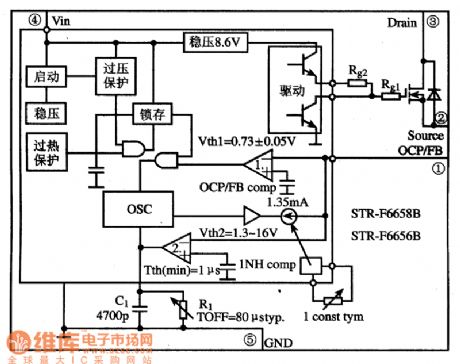
High-speed current driver composed of two OPA660 (wideband transconductance op amp and buffer)
Published:2012/8/15 1:02:00 Author:Ecco | Keyword: High-speed , current driver , wideband transconductance, op amp, buffer
The circuit usestwo OPA660 to form a push-pull circuit to increase the output current, and it can be used to drive the load such as magnetic head and so on.
(View)
View full Circuit Diagram | Comments | Reading(1172)
Differential input maintaining circuit composed of two LF198 sample maintainging amplifiers
Published:2012/8/15 1:53:00 Author:Ecco | Keyword: Differential , input, maintaining circuit, sample, maintainging amplifiers
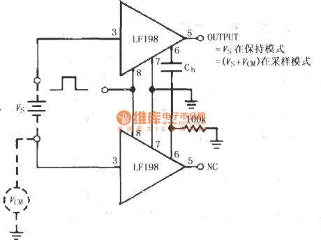
The purpose of using two LF198is to usesymmetry of the circuit to eliminate the impact on circuit from the common-mode voltage and keepthe output Vs ( does not contain VCM ) inmaintaining mode.
(View)
View full Circuit Diagram | Comments | Reading(827)
Data acquisition system grounding and coupling circuit ( sample maintaining amplifier AD783 )
Published:2012/8/15 1:55:00 Author:Ecco | Keyword: Data acquisition system, grounding , coupling , sample maintaining , amplifier
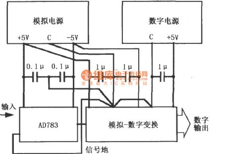
As a high-speed, high - resolution data acquisition syste , power supply must be well regulated to control additional high-frequency noise (ripple). AD783 power connection in figure can well meet above requirements, while enable to transmit instantaneous current to the device.
(View)
View full Circuit Diagram | Comments | Reading(699)
Typical data acquisition system grounding and coupling circuit (AD781/AD674)
Published:2012/8/15 2:01:00 Author:Ecco | Keyword: Typical , data acquisition system , grounding , coupling circuit
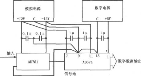
As a high-speed, high - resolution data acquisition syste , power supply must be well regulated to control additional high-frequency noise (ripple). AD781 power connection in figure can well meet above requirements, while enable to transmit instantaneous current to the device. In order to achieve the rated accuracy and dynamic performance, the power supply decoupling capacitors must be directly connected between the positive power supplyfeet and the negative feet to ground, and typically itconnects 0.1μF ceramic capacitorsbetween VCC and VEE to ground.
(View)
View full Circuit Diagram | Comments | Reading(598)
DC and AC zeroing circuit of sample maintaining amplifier LF398
Published:2012/8/15 2:05:00 Author:Ecco | Keyword: DC and AC , zeroing circuit, sample maintaining, amplifier
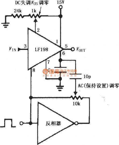
Adjusting 1kΩ potentiometer can makeDC offset voltage Vos be zero. In maintaining set mode, adjusting the 10kΩ potentiometer allows the AC offset voltage Vosto bezero.
(View)
View full Circuit Diagram | Comments | Reading(1106)
Quasi - synchronous decimal counter circuit
Published:2012/8/15 2:39:00 Author:Ecco | Keyword: Quasi - synchronous , decimal counter
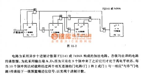
The circuit is adder circuit composed of asynchronous decimal counter FJJ141 or the 7490A. All levels'data is transferred by decoding circuit. So output ends A , D are in high level only after nine pulses comes. Once two pulses arrive, they will be transferred to next preset end for carrying signal by two interconnected gates ( gate 1 and 2, or gate 1 and a corresponding NAND gate ), then the circuit realizes the decimal counting.
(View)
View full Circuit Diagram | Comments | Reading(781)
Typical data acquisition system grounding and coupling circuit (AD684/AD674)
Published:2012/8/15 1:59:00 Author:Ecco | Keyword: Typical, data acquisition system , grounding , coupling circuit
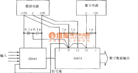
As a high-speed, high - resolution data acquisition syste , power supply must be well regulated to control additional high-frequency noise (ripple). AD684 power connection in figure can well meet above requirements, while enable to transmit instantaneous current to the device. In order to achieve the rated accuracy and dynamic performance, the power supply decoupling capacitors must be directly connected between the positive power supplyfeet and the negative feet to ground, and typically itconnects 0.1μF ceramic capacitorsbetween VCC and VEE to ground.
(View)
View full Circuit Diagram | Comments | Reading(768)
High-speed current driver composed of two wideband transconductance op amp and buffer OPA660
Published:2012/8/15 0:54:00 Author:Ecco | Keyword: High-speed, current, driver , wideband transconductance, op amp, buffer
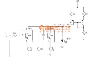
The circuit uses two OPA660 connected in parallel to increase the output current. The transistors Q1, Q2form image constant current source circuit, which are used asthe collector load of two parallel OPA660. Q1, Q2 are selected 2N3906.
(View)
View full Circuit Diagram | Comments | Reading(1478)
The basic application circuit of photodiode (optical signal amplifier, switching circuits)
Published:2012/8/15 0:57:00 Author:Ecco | Keyword: basic application , photodiode , optical signal amplifier, switching circuits)
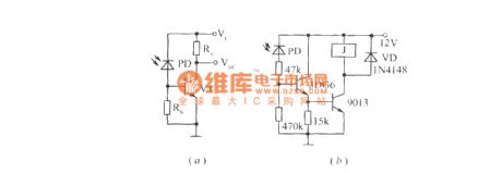
As shown in figures, ( a ) shows light signal amplifier circuit composed of photodiode; (b) shows the switching circuit composed of photodiode.
(View)
View full Circuit Diagram | Comments | Reading(1208)
Laser torch schematic
Published:2012/8/15 20:45:00 Author:Ecco | Keyword: Laser torch, schematic
Laser torch is cheap and has high cost performance. The main feature is the excellent performance of the condenser, and the optical rangeis up to 1200m ~ 1500m, and the spot is still small from a few hundred meters in visual observation, so it is widely used in teaching , guided tours and entertainment. According to tests, it can be used for long-distance of the protective guard and the remote data transmission. Laser torch schematic is shown in Fig, the components are SMD components, so the device is small, and the power of laser is great, it can not direct shoot the human eye.
(View)
View full Circuit Diagram | Comments | Reading(2392)
The current reference temperature compensation circuit of logarithm and logarithmic ratio amplifier LOG100
Published:2012/8/13 21:24:00 Author:Ecco | Keyword: current reference, temperature compensation , logarithm , logarithmic ratio amplifier
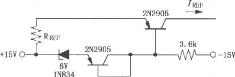
If I2 = IREF is set as a constant, IREF is the reference current, the output voltage VOUT = KlogI1/IREF , IREF= 6V/RREF. The figure is IREF's current source circuit generated by the external circuit, the circuit uses 6V 1N834 zener regulator which is connected to 2N2905 transistor's emitter junction in reverse series to make the temperature compensation and improve thetemperature stability of output reference current IREF.
(View)
View full Circuit Diagram | Comments | Reading(1921)
| Pages:87/471 At 2081828384858687888990919293949596979899100Under 20 |
Circuit Categories
power supply circuit
Amplifier Circuit
Basic Circuit
LED and Light Circuit
Sensor Circuit
Signal Processing
Electrical Equipment Circuit
Control Circuit
Remote Control Circuit
A/D-D/A Converter Circuit
Audio Circuit
Measuring and Test Circuit
Communication Circuit
Computer-Related Circuit
555 Circuit
Automotive Circuit
Repairing Circuit