
Index 128
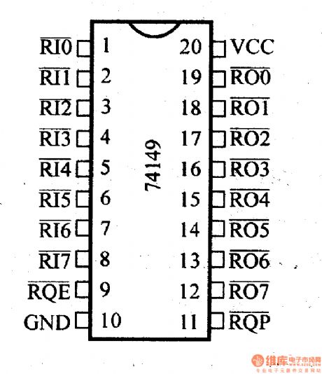
74 Series digital circuit of 74HC149 8-8 line priority encoder
Published:2011/8/1 20:54:00 Author:Lucas | Keyword: 74 Series , digital circuit, 8-8 line priority encoder
View full Circuit Diagram | Comments | Reading(1969)
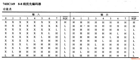
74 Series digital circuit of 74142 BCD counter / 4-bit latch / BCD decoder / driver
Published:2011/7/25 3:14:00 Author:Lucas | Keyword: 74 Series, digital circuit , BCD counter, 4-bit latch, BCD decoder, BCD driver
All other outputs are off.
It contains a BCD counter, a 4-bit latch and a decoder, Nixie tube driver; the counter accepts input clock frequency which is up to 20MHZ; driver tube has the same input with 74141.
(View)
View full Circuit Diagram | Comments | Reading(3501)
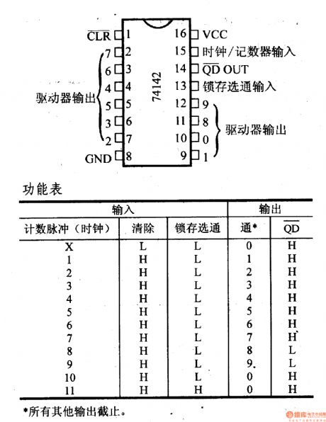
74 Series digital circuit of 74141 BCD decimal decoder / driver
Published:2011/7/25 3:14:00 Author:Lucas | Keyword: 74 Series , digital circuit , BCD decimal decoder, BCD decimal driver
It can drive inflated cold-cathode display tube directly; all decoding input could ensure that all outputs of invalid code are off; the maximum reverse current of NPN output transistor is 50mA whenunder 55V.
(View)
View full Circuit Diagram | Comments | Reading(2014)
Power drive circuit with 180°output phase differencebetween normal and opposite phase
Published:2011/7/25 3:08:00 Author:Lucas | Keyword: Power drive circuit , 180°, output phase difference , normal , opposite phase
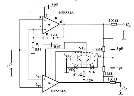
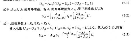
If the common emitter current of VTl and the two transistors in the first differential amplifier circuit composed of A2 chip are equal, then the following equation is effective, Av2 is the open-loop gain of A2. If the open-loop gain of A1 is AV1, then the positive phase output U01, feedback factor, input voltage can be gotten by the following equations. Comparing with the equations (2-2) and (2-3), if A (V1) = A (V2), the U. 1/Ui and U. 2/Ui have the same frequency characters. For any frequency, the normal-phase output U. l and the inverted output U. 2 have 180 °phase difference.
(View)
View full Circuit Diagram | Comments | Reading(854)
74 Series digital circuit of 74LS320 crystal-controlled oscillator
Published:2011/8/1 20:51:00 Author:Lucas | Keyword: 74 Series , digital circuit, crystal-controlled oscillator
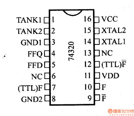
The working frequency range of crystal-controlled oscillator/ clock pulse is 1Hz ~ 20MHz; TTL level and high level(5V-12V) have 2-phase output.
(View)
View full Circuit Diagram | Comments | Reading(1139)
74 Series digital circuit of 74283,74LS283 4-bit binary full adder (with carry lookahead)
Published:2011/8/1 20:52:00 Author:Lucas | Keyword: 74 Series , digital circuit , 4-bit binary , full adder , carry lookahead
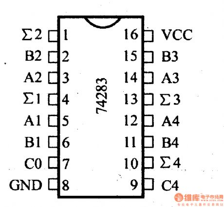
The functions are similar to 7483A, 74LS83A, and the table is same with the 7483A.
(View)
View full Circuit Diagram | Comments | Reading(15797)
74 Series digital circuit of 74S281 4-bit parallel binary accumulator
Published:2011/8/1 20:52:00 Author:Lucas | Keyword: 74 Series, digital circuit , 4-bit parallel , binary accumulator
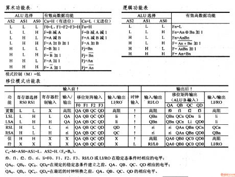
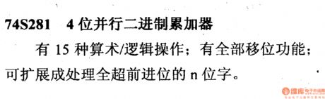
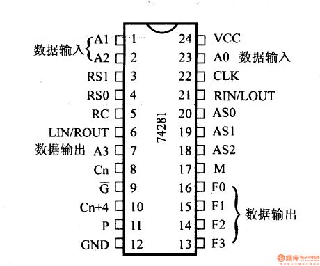
There are 15 arithmetic, logical operations; it has a full shift function; it can be extended full-ahead position N-bit words.
fo, f1, f2,f3 = the corresponding steady input level of F1, F2, F3, F4. QA0, QB0, QC0, QD0= the corresponding level of QA, QB, QC, QD before the establishment of steady-state input conditions. QAn, QBn, QCn= the corresponding level of QA, QB, QC at the latest time hopping.
(View)
View full Circuit Diagram | Comments | Reading(1837)
74 Series digital circuit of 74LS258,74F258 four 2-to-1 data selector (tristate, inverted)
Published:2011/8/9 3:29:00 Author:Lucas | Keyword: 74 Series , digital circuit , four 2-to-1 , data selector , tristate , inverted
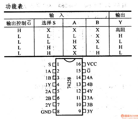
Tristate output is connected to the system bus interface directly, and 74LS258A absorption current is twice large than the 74LS258.
(View)
View full Circuit Diagram | Comments | Reading(1278)
74 Series digital circuit of 74LS242/243 four-bus transceiver (tristate) / line driver
Published:2011/8/9 3:30:00 Author:Lucas | Keyword: 74 Series, digital circuit , four-bus transceiver , tristate , line driver

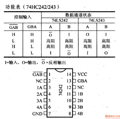
It can make dual-channel asynchronous communication between the data bus; the state of the control input determines the direction of data flowing and the data port model; 242 is the tri-state inverting output, and 243 is the three-state in-phase output. If the transceiver is allowed in both directions at the same time, it may occur destructive oscillation.
(View)
View full Circuit Diagram | Comments | Reading(1387)
74 Series digital circuit of 74LS240,74F240 eight inverting buffer/line driver/ line receiver(three-state)
Published:2011/8/1 20:52:00 Author:Lucas | Keyword: 74 Series , digital circuit , eight inverting buffer, line driver, line receiver, three-state
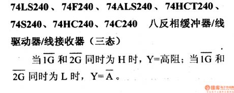
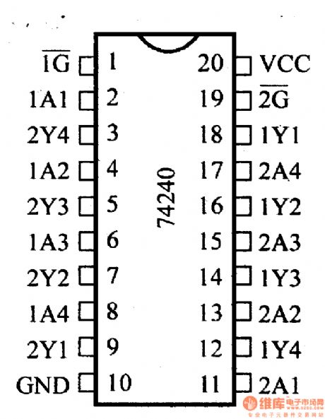
When 1G and 2G are H at the same time, Y=high resistance;when 1G and 2G are L at the same time, Y=A.
(View)
View full Circuit Diagram | Comments | Reading(1224)
74 Series digital circuit of 74199 8-bit shift register
Published:2011/8/1 20:52:00 Author:Lucas | Keyword: 74 Series , digital circuit, 8-bit shift register
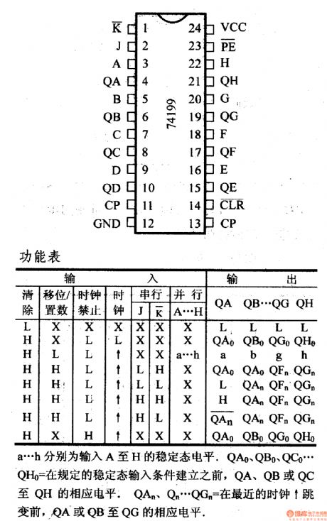

Parallel storage; right shift(direction is from the QA to QH): left shift(direction is from the QH to QA); it forbids the clock.a. .. h= the input of steady-state input level of A to H.QAo, QBo, QGo, QHo=the corresponding level level of QA, QB, QG, QH before building the specified steady state.QAn, QBn..QGn= the corresponding level of QA, QB to QGbefore the next jump of the clock.
(View)
View full Circuit Diagram | Comments | Reading(1378)
74 Series digital circuit of 74196/74197 preset decimal/binary counter
Published:2011/8/1 20:53:00 Author:Lucas | Keyword: 74 Series, digital circuit , preset decimal counter, binary counter
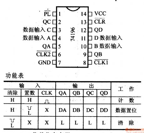
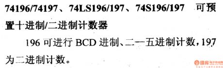
196 can make BCD binary/quinary count, and 197 is the binary counter.
(View)
View full Circuit Diagram | Comments | Reading(1951)
74 Series digital circuit of 74160/161/162/16 synchronous 4-bit counter
Published:2011/8/1 20:53:00 Author:Lucas | Keyword: 74 Series , digital circuit , synchronous 4-bit counter
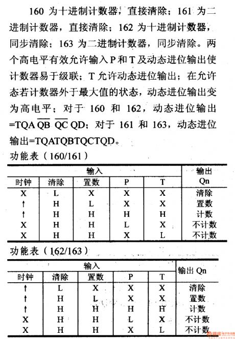
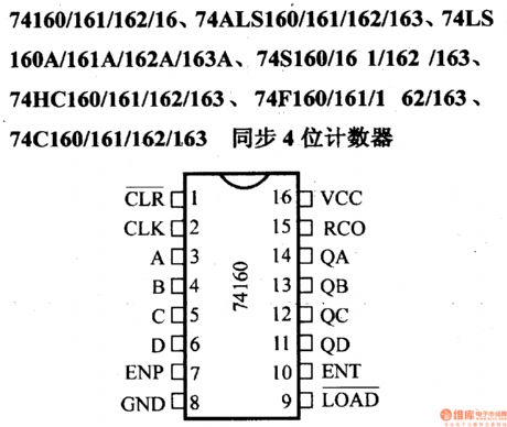
160 is the decimal counter, which can direct remove; 161 is the binary counter, which can direct remove; 162 decimal counter can synchronous clear; 163 binary counter can synchronous clear. Two active-high inputs P and T allow dynamic counter to be easy to carry out the cascade; T allows dynamic binary output; if the counter is at a maximum state in the allowing state, the dynamic binary output will go high.
(View)
View full Circuit Diagram | Comments | Reading(3391)
Voltage-controlled oscillator (NE566V) circuit can be controlled in the wide range
Published:2011/8/8 8:03:00 Author:nelly | Keyword: Voltage-controlled, oscillator, wide range
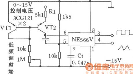
Voltage-controlled oscillator (NE566V) circuit can be controlled in the wide range . (View)
View full Circuit Diagram | Comments | Reading(832)
The circuit diagram of high precision and low offset current follower (LM11C, LF351)
Published:2011/8/8 22:11:00 Author:Felicity | Keyword: high precision, low offset, current follower
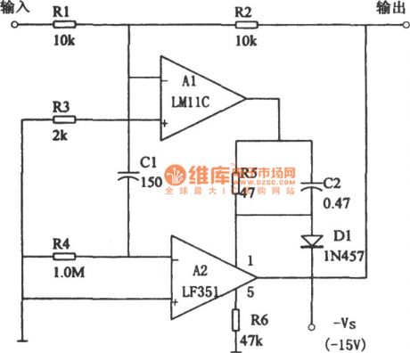
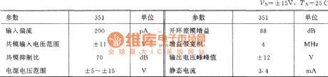
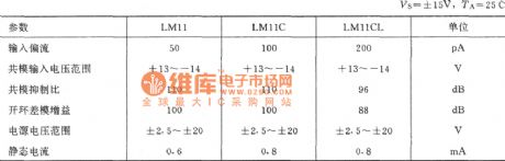
LM11C has a very low offset current (around 100pA), a low misalignment voltage( around 0.6 mV) and a 110dB CMRR.LF351 operational amplifier has a misalignment voltage about 10mv ,a static current around 3.4mA and a input offset current about 200PA. In this circuit, A2 adopts alternating-current coupling to reduce offset current. And this circuit has a long overload recovery time and the common-mode input voltage cannot exceed ±l0V. (View)
View full Circuit Diagram | Comments | Reading(988)
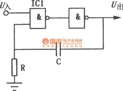
monostable trigger circuit formed by gate circuit
Published:2011/7/22 3:01:00 Author:chopper | Keyword: monostable trigger, gate circuit
The CMOSnand-gate ornor-gate can form a monostable trigger, and this monostable trigger is used for the delay,broadening and shaping of the pulse signal extensively in the circuit.The main principle of monostable trigger with a gate circuit is to use the charge and discharge actions of the threshold level of gate input end and the component RC added to the gate circuit.Bothnand-gate or logic gate can form the monostable trigger,but their trigger modes are different,and the output logic levels are also different
.
(View)
View full Circuit Diagram | Comments | Reading(1022)
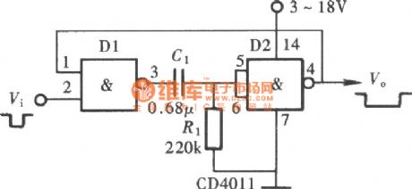
slack delay monostable trigger with nand-gate
Published:2011/7/22 3:00:00 Author:chopper | Keyword: slack delay, monostable trigger, nand-gate
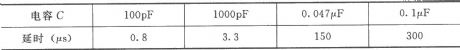
The picture shows aslackdelay monostable trigger with negative pulse trigger,and it provides a few seconds delay time for timing the situation whose accuracy is not critical. The delay in picture is mainly determined by capacitor C.As for TTL circuit,the resistance of R is generally 5~10kΩ. The table lists the measured data of delay when R = 5.1kΩ.The maximum capacity of C can reach several hundred microfarads, and delay can up to a few seconds.
(View)
View full Circuit Diagram | Comments | Reading(1562)
74 Series digital circuit of 74LS395A,74F395 4-bit cascadable shift register (tristate)
Published:2011/8/1 22:50:00 Author:Lucas | Keyword: 74 Series , digital circuit , 4-bit cascadable, shift register , tristate
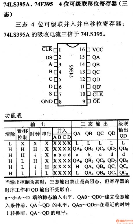
It is the tri-state 4-bit cascaded parallel input and output shift register; 74LS395A absorption current is three times greater than 74LS395. When output control is high, the tri-state output disable is high impedance, but the timing work and QD output of the register is not affected.
a~ d = the corresponding steady input level of A~ D. QA0~ QD0= the corresponding level of QA~QD before the establishment of steady-state input conditions. QAn~ QDn= the corresponding level of QA~ QD at the latest time hopping.
(View)
View full Circuit Diagram | Comments | Reading(1290)
74 Series digital circuit of 74LS384, 74F384 8-bit × 1-bit complement multiplier
Published:2011/8/2 1:00:00 Author:Lucas | Keyword: 74 Series , digital circuit , 8-bit × 1-bit , complement multiplier
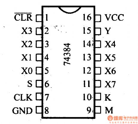
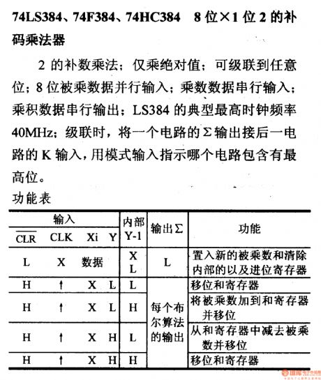
2's complement multiplication; it is only multiplied by the absolute value; it can be cascaded to any bit; 8-bit multiplied data parallel input; multiplier data serial input; product data serial output; LS384 typical maximum clock frequency is 40MHz; when is is cascaded,the output of a circuit is connected to K input of the next circuit, and the circuit contains the highest level can be indicated by the model input.
(View)
View full Circuit Diagram | Comments | Reading(1811)
74 Series digital circuit of 74LS373, 74ALS373 octal D-latch(tristate)
Published:2011/8/1 23:01:00 Author:Lucas | Keyword: 74 Series , digital circuit , octal D-latch, tristate
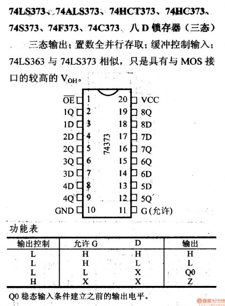
Tristate output; the load full parallel access; buffer control input; 74LS363 is similar to 74LS373, but has the high VOH with MOS interface.
Q0 = the output level before establishing the steady-state input conditions.
(View)
View full Circuit Diagram | Comments | Reading(5363)
| Pages:128/471 At 20121122123124125126127128129130131132133134135136137138139140Under 20 |
Circuit Categories
power supply circuit
Amplifier Circuit
Basic Circuit
LED and Light Circuit
Sensor Circuit
Signal Processing
Electrical Equipment Circuit
Control Circuit
Remote Control Circuit
A/D-D/A Converter Circuit
Audio Circuit
Measuring and Test Circuit
Communication Circuit
Computer-Related Circuit
555 Circuit
Automotive Circuit
Repairing Circuit