
Index 135
AFSK_KEYER
Published:2009/7/14 23:55:00 Author:Jessie
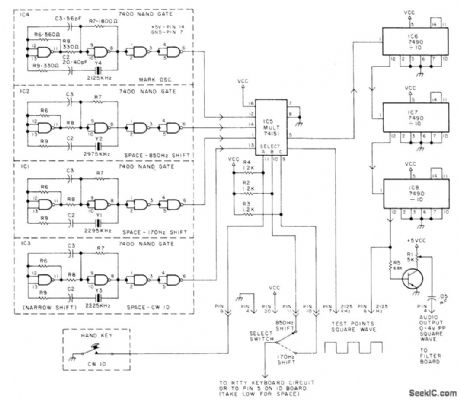
Developed for use with 49.MHz FM transmitter to rebroadcast hurricane bulletins and other weather warnings to amateur RTTY stations. Crystals assure high precision in generating RTTY tones for 850-Hz shift, with extra clystals for 170-Hz shift and for narrow-shift CW identification. Frequency tolerance is ±1 Hz and requires no calibration. Circuit uses 7400 quad NAND-gate crystal oscillator, which works with almost any HC-6/U crystal. Frequency can be adjusted by changing value of C2. Outputs feed 74151 multiplexer. When all SELECT inputs are high (2.8-5 V), mark oscillator frequency appears at multiplexer output. When input B is low (0-0.8 V), multiplexer output changes to space frequency of 2975 kHz, Multiplexer feeds divide-by-1000 chain feeding 2125-Hz square wave to buffer transistor. Article gives circuit of low-pass filter that removes harmonics from output to give pure sine wave for modulating transmitter.-L. J. Fox, Dodge That Hurricane!, 73 Magazine, Jan. 1978, p 62-69. (View)
View full Circuit Diagram | Comments | Reading(1650)
CERAMIC_CARTRIDGE_PHONO_PREAMP
Published:2009/7/14 23:52:00 Author:Jessie
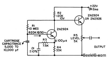
Gives RIAA equalized output. With Astatic model 137 cartridge, output reference level of 1 v is 13 db below maximum output and 69 dbabove unweighted noise level.- Transistor Manual, Seventh Edition, General ElectricCo.,1964,p 258. (View)
View full Circuit Diagram | Comments | Reading(4283)
BASIC_4_TRANSISTOR_PHANTASTRON
Published:2009/7/14 23:52:00 Author:Jessie
Article traces operation and analyzes sources of timing errors.-S. R. Parris and D. A. Staar, Highly Accurate Phantastron Delay Circuit, Electronics, 33:43, p72-74. (View)
View full Circuit Diagram | Comments | Reading(865)
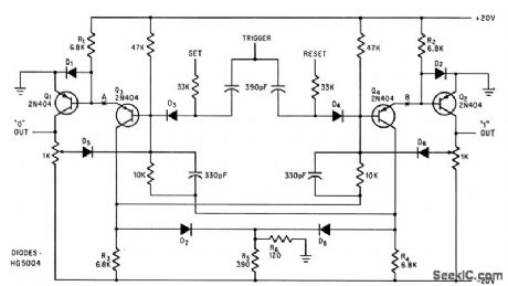
TUNNEL_DIODE_FUP_FLOP
Published:2009/7/14 21:08:00 Author:May
Power consumption is very low. Takes advantage of fast switching speed (27 picosec) of tunnel diode.- Transistor Manual, Seventh Edition, General Electric Co., 1964, p 367. (View)
View full Circuit Diagram | Comments | Reading(788)
STEPPED_TRIANGLE_WAVEFORM_GENERATOR
Published:2009/7/14 23:51:00 Author:Jessie
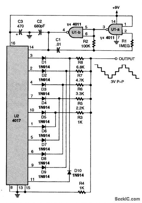


An astable multivibrator (made up of U1-a and U1-b) drives a 1-of-10 counter. A resistor matrix acts as a rough D-A converter and produces the stepped triangle waveform shown. The waveform can be tailored to suit by adjusting R3,through R8 (View)
View full Circuit Diagram | Comments | Reading(1859)
SCR_UJI_TIME_DELAY
Published:2009/7/14 23:50:00 Author:Jessie
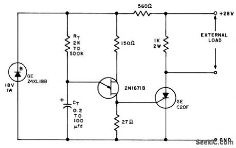
Timing interval is initiated by applying power, and is determined by RT-CT. At end of interval, unijunction transistor triggers silicon controlled rectifier, to apply essentially full supply voltage to load. Delay range is from 0.4millisec to 1 minute.- Transistor Manual, Seventh Edition, General Electric Co.1964, p 321. (View)
View full Circuit Diagram | Comments | Reading(852)
DELAY_MULTIPLIER
Published:2009/7/14 23:48:00 Author:Jessie
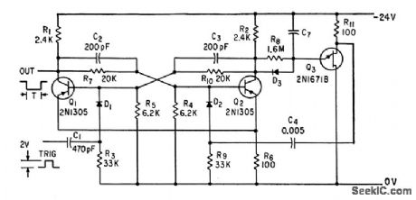
Addition of silicon unijunction transistor Q3 to conventional mono stable mvbr expands time delay two orders of magnitude.-M. P. Humblet, Unijunction Transistor Multiplies Monostable 's Pulsewidth, Electronics, 35:26, p 74-75. (View)
View full Circuit Diagram | Comments | Reading(787)
HARMONIC_GENERATOR
Published:2009/7/14 23:47:00 Author:Jessie
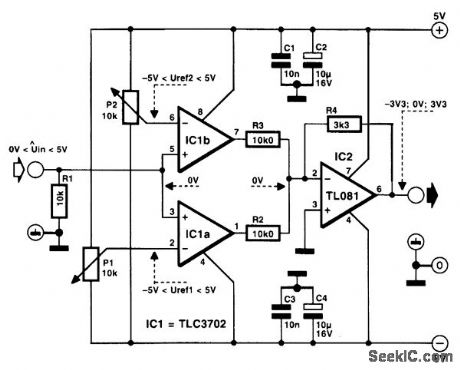
This simple circuit acts as a frequency multiplier, which converts any sloped input waveform into a distorted output waveform, whose frequency spectrum is marked by a rich harmonics content.The input frequency does not disappear from the spectrum, however. When a pure sine-wave input signal is applied, the circuit generates odd harmonics only. The push-pull outputs of comparators IC1b and IC1a then supply differential signals to adder IC2, which cancels out even-numbered harmonics. For different mark/space ratios of the output signals, as set with P1 and P2, the harmonic spectrum changes. A duty factor of 0.25, for instance, will cause the circuit to supply the second, sixth, and tenth harmonics, but not the fourth one. The spectrum function is then written as sin x/x.The reference levels for the input comparators determine the output waveform. The desired degree of distortion of the input waveform is, therefore, adjusted with the two presets. R2 and R3 should be matched to within 1 percent. (View)
View full Circuit Diagram | Comments | Reading(3792)
BYPASSING_SOLENOID_TRANSIENTS
Published:2009/7/14 23:46:00 Author:Jessie
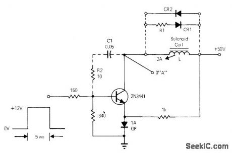
Feedback from collector to base of power transistor through C1 and R2 protects device from destructive transients generated when inductive load such as solenoid is turned off. Alternative use of diode CR2 or CR1-R1 across coil would limit voltage transient but would increase solenoid release time.-D. Thomas, Feedback Protects High-Speed Solenoid Driver, EDN Magazine, Jan. 1, 1971, p 40.
(View)
View full Circuit Diagram | Comments | Reading(1026)
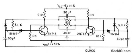
250_KC_FLIP_FLOP
Published:2009/7/14 21:05:00 Author:May
Basic design procedure is given. Circuit shown operates over temperature range of -55 to +55℃ with input frequency of 250 kc.-Texas Instruments Inc., Transistor Circuit Design, McGraw-Hill, N.Y., 1963, p 377. (View)
View full Circuit Diagram | Comments | Reading(844)
MULTCHIP_COMPLEMENTARY_FLIP_FLOP
Published:2009/7/14 21:04:00 Author:May


Circuit for microelectronic application allows use of most suitable substrate for each component.-J. Eimbinder, Multichip Circuits Get Off The Ground, Electronics, 37:25, p105-107. (View)
View full Circuit Diagram | Comments | Reading(742)
NONSATURATED_FLIP_FLOP
Published:2009/7/14 21:00:00 Author:May
Design procedure is given in 52 steps for manufacturability and long-term reliability, making full allowance for component tolerances, voltage fluctuation, and collector output loading.- Transistor Manual, Seventh Edition, General Electric Co., 1964, p 189. (View)
View full Circuit Diagram | Comments | Reading(762)
FAN_OUT_TO_60
Published:2009/7/14 20:59:00 Author:May
Fan-out of conventional flip-flop is quadrupled by driving bases of amplifiers Q1 and Q2 directly from emitters of Q3 and Q4.-D. J. Grover, Modified Flip-flop Quadruples Fan-Out, Electronics, 38:26, p 67-68. (View)
View full Circuit Diagram | Comments | Reading(678)
UART_INTERFACE
Published:2009/7/14 23:43:00 Author:Jessie
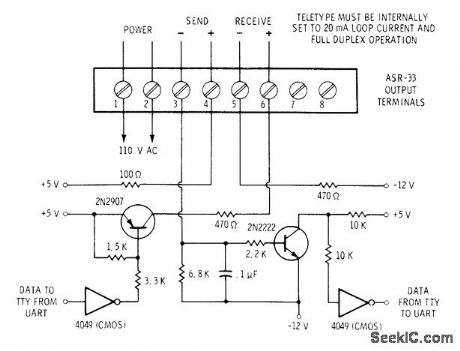
Permits use of universal asynchronous receiver-transmitter with model 33 Teletype so keyboard can send and printer can receive at same time. Transmitter interface provides 20-mA current for mark or 1 and open circuit for space or 0. Receiver senses closed contact for mark or 1 and open contact for space or 0. Extra inverters are added to make codes correspond so 1 from UART is read as 1 by Teletype. Designed for 110-baud rate.-D. Lancaster, TV Typewriter Cookbook, Howard W. Sams, Indianapolis, IN, 1976, p 162-164. (View)
View full Circuit Diagram | Comments | Reading(0)
PROGRAMMABLE_PULSE_GENERATOR
Published:2009/7/14 23:43:00 Author:Jessie
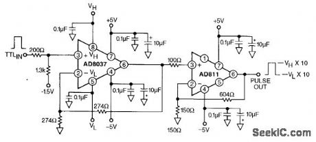
This circuit provides a programmable flat-pulse generator with TTL input and up to 24 V p-p output with a 2500-V-μs slew rate. Clamp amplifiers are useful as protective buffers for A/D inputs, as programmable flat-pulse-forming amplifiers, and as amplitude modulators. Because VH and VL clip in the in-put stage and have input bandwidths comparable to the signal inputs, they can also be used in simple circuitry to generate the positive or negative absolute value of input signals (i.e., full-wave rectify them). (View)
View full Circuit Diagram | Comments | Reading(1843)
FAIL_SAFE_INTERLOCK
Published:2009/7/14 23:43:00 Author:Jessie
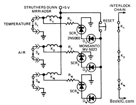

Developed for protecting people and equipment at 40-kW RF accelerator station. All interlock switches (air flow, water flow, water pressure, temperature, etc) are normally closed, grounding one side of each relay coil. All relays are normally pulled in, to provide complete interlock chain. Failure of any component, including power supply, breaks chain and places system in safe mode.-T. W. Hardek, Interlock Protection Circuit Is Simple and Fail-Safe, EDN Magazine, May 20, 1975, p 74. (View)
View full Circuit Diagram | Comments | Reading(1407)
TUNNEL_DIODE_COUPLED__MICROENERGYFLIP_FLOP
Published:2009/7/14 20:56:00 Author:May
Fan-in and fan-out capabilities per unit dissipation are improved up to ten times over existing types of logic. Use of tunnel diodes allows low supply voltages, resulting in low circuit dissipation.-T. Maguire, Electro-Optical Developments Highlight NEREM, Electronics, 34:45, p 73-77. (View)
View full Circuit Diagram | Comments | Reading(676)
SINGLE_ENDED_CLASS_B_OUTPUT
Published:2009/7/14 23:41:00 Author:Jessie
High-fidelity 10-w amplifier uses capacitor and diodes to couple class A driver,to single-ended class B output feeding 16-ohm speaker. Input stages are equalized for RIAA curve. Frequency response is flat within 1.5 db from 30 to 15,000 cps.-H.C.Lin and B.H.White,Single-Ended Amplifiers for Class B Operation Electronics,32:22,p 86-87. (View)
View full Circuit Diagram | Comments | Reading(1318)
TRIANGLE_WAVEFORM_GENERATOR
Published:2009/7/14 23:41:00 Author:Jessie
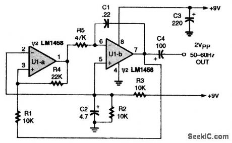
A low-frequency triangle-waveform generator is made from a single LM158 dual op amp and a few inexpensive components. The output frequency can be varied by changing the R5, Changing the value of C1, will shift the circuit's frequency range: Increasing the value will lower the oscillator's frequency and reducing the value will increase the frequency. Resistor R4 can be varied to change the output level. Powered from a 9-V supply, the circuit produces a 2-V p-p triangular output waveform. (View)
View full Circuit Diagram | Comments | Reading(1180)
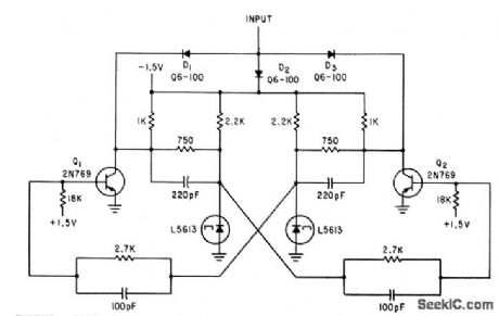
WIDE_TEMPERATURE_RANGE
Published:2009/7/14 20:55:00 Author:May
Gives 10-Mc op eration from -55℃ to +125℃, with 3.v dock trigger. Addition of emitter-follower will improve wove form and extend operation to +150℃.-D. Hall, Using Epitaxial Transistors in Switching and R-F Circuits, Electronics, 34:13, p 52-53. (View)
View full Circuit Diagram | Comments | Reading(733)
| Pages:135/471 At 20121122123124125126127128129130131132133134135136137138139140Under 20 |
Circuit Categories
power supply circuit
Amplifier Circuit
Basic Circuit
LED and Light Circuit
Sensor Circuit
Signal Processing
Electrical Equipment Circuit
Control Circuit
Remote Control Circuit
A/D-D/A Converter Circuit
Audio Circuit
Measuring and Test Circuit
Communication Circuit
Computer-Related Circuit
555 Circuit
Automotive Circuit
Repairing Circuit