
Basic Circuit
Index 44
1 KW Power (Watt) Meter circuit
Published:2013/3/29 4:28:00 Author:Ecco | Keyword: 1 KW , Power (Watt) Meter
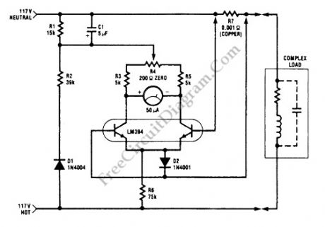
This watt-meter circuit has measurement range up to 1-KW. This circuit can give the complete (X)(Y) function although uses only one transistor. Actually, this circuit is used for 117 Vac±50 Vac operation. For lower or lower voltage, this circuit can be modified easily. This circuit only measure power on negative cycles. The advantages of this circuit is this circuit does not need external power supply. This circuit measures true power that is delivered to the load. Here is the schematic diagram of the circuit:
(View)
View full Circuit Diagram | Comments | Reading(1998)
Direct High Voltage DC Regulator circuit
Published:2013/3/29 4:26:00 Author:Ecco | Keyword: Direct, High Voltage, DC Regulator
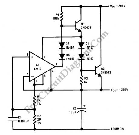
This regulator circuit stabilize the output voltage at 200V directly (without a transformer). Although the output voltage is high, this circuit only suffer a tension of the voltage drop (Vinput-Voutput), which is suffered mainly by the transistors. The op-amp suffers even less tension, since it regulate the applied voltage at their pins around the level of transistor’s bias voltage level.
(View)
View full Circuit Diagram | Comments | Reading(1959)
Funk (Twang) Guitar Effect Box circuit
Published:2013/3/29 4:25:00 Author:Ecco | Keyword: Funk (Twang) Guitar Effect Box
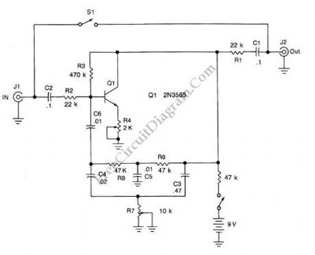
This is an audio effect circuit that give extra oscillation to your guitar, percussive, or semi percussive instruments, you can call it a funk box. This guitar effect circuit is basically a damped oscillator that is set slightly below its critical oscillation point. The oscillator part is constructed by feeding back the output signal through a bandpass circuit, with the center frequency is adjusted by potentiometer R7 to add an extra “twang” , adjustable from low to high pitched timbre. Potentiometer R4 is used to adjust the gain of the oscillator, should be set to damp the oscillation at the desired decay time. To adjust it, turn the knob slowly until a steady oscillation occurs, and turn back slightly just before it happens (the oscillation should ceases slowly). Here is the schematic diagram of the circuit:
(View)
View full Circuit Diagram | Comments | Reading(1540)
Versatile Discrete Monostable Multivibrator
Published:2013/3/28 4:15:00 Author:Ecco | Keyword: Versatile Discrete, Monostable Multivibrator
This is a versatile discrete monostable circuit. This circuit consist of 2N3819 JFET and 2N3704 transistors. This monostable multivibrator circuit has additional input to enable or inhibit the function at any time without causing output pulse. The input of this circuit accept a standard digital IC voltage levels. Here is the schematic diagram of the circuit:
(View)
View full Circuit Diagram | Comments | Reading(2334)
Optical Theremin
Published:2013/3/28 4:13:00 Author:Ecco | Keyword: Optical Theremin
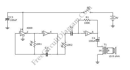
Normally, Theremin works by detecting hand proximity using capacitive coupling method. A Theremin circuit shown in the schematic diagram below use different method to control the pitch. The oscillator of this tone generator, both the volume and frequency are controlled using LDRs, a light sensitive electronic component, so we can call this circuit an optical Theremin. Look at the following schematic diagram:
(View)
View full Circuit Diagram | Comments | Reading(2655)
Tachometer Circuit Diagram with Single Transistor
Published:2013/3/28 4:10:00 Author:Ecco | Keyword: Tachometer , Single Transistor
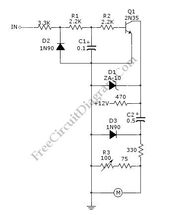
A schematic diagram of simple tachometer circuit is shown below. Using only a single transistor as the active component, this tachometer would probably be the simplest one. The input of this circuit can be picked up from ignition pickup coil, or other wiring that gives ignition wave-form. This tachometer circuit works for 0 to 6,000 rpm. R3 is used for calibrating the full scale meter reading, to get valid rpm. The zener diode D1 is used to stabilize the 12-V supply. Here is the schematic diagram of the circuit:
(View)
View full Circuit Diagram | Comments | Reading(1469)
Direct Coupled Discrete Astable Multivibrator circuit
Published:2013/3/28 4:04:00 Author:Ecco | Keyword: Direct Coupled Discrete, Astable Multivibrator
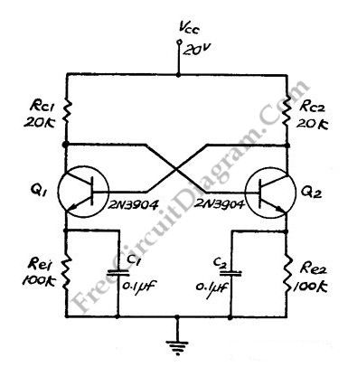
This flip-flop circuit is a free running/astable multivibrator one, with bases and collector of both emitter biased transistor are directly coupled to each other. Switching action is supported by means of capacitor in each emitter circuit. This configuration produce a triangle waves at emitters. Since neither transistor can remain permanently cut off, then a free running oscillation will be generated. We can use single 0.1 uF capacitor between emitters in place of C1 and C2.
(View)
View full Circuit Diagram | Comments | Reading(2240)
AD532 Multiplier IC diagram and Its Pin Configurations
Published:2013/3/28 4:04:00 Author:Ecco | Keyword: Multiplier IC
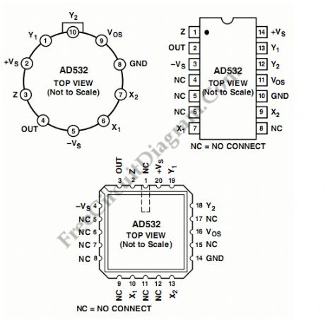
The AD532 is the first pre-trimmed single chip monolithic multiplier/divider. This device guarantees a maximum multiplying error of +- 1% and a +-10 V output voltage without the need for any output op amp or external trimming resistors. It’s simplicity of use provides design engineers with an attractive alternative to modular multipliers because the AD532 is internally trimmed. The AD532 is monolithic construction provides significant advantages in size, reliability and economy. The AD532 also can be used as a direct replacement for other IC multipliers that require external trim network. This device can be applied on various application such as power measurement, multiplication, division, squaring, square rooting, algebraic computation and instrumentation applications. The AD532 also available in chip form.
(View)
View full Circuit Diagram | Comments | Reading(1063)
Single Chip Circuit diagram for Multiplication Operation
Published:2013/3/28 4:03:00 Author:Ecco | Keyword: Single Chip , Multiplication Operation
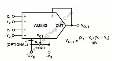
The AD532 should be connected as the following figure for operation as a multiplier. We can fed the input differentially to the X and Y inputs, or single ended by simply grounding the unused input. Connect the inputs according to the desired polarity in the output. To close the feedback loop around the op amp, the Z terminal is tied to the output. The offset adjust Vos is optional and is adjusted when both inputs are zero volts to obtain zero out, or to buck out other system offsets.
(View)
View full Circuit Diagram | Comments | Reading(694)
The square Root Mode for AD532 Analog Processor
Published:2013/3/28 4:00:00 Author:Ecco | Keyword: Square Root Mode, Analog Processor
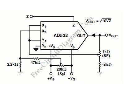
The following schematic diagram shows us about the connections for square root mode for ADS532 analog processor chip. Similar to the division mode, the multiplier cell is connected in the feedback of the op amp by connecting the output back to both the X and Y inputs. To prevent latch up as Zi approaches 0 Volts, the diode D1 is connected. The Vov adjustment is made with Zin = +0.1 V dc in this case, adjusting Vos to obtain -1.0 V dc in the output, Vout =-√(10 VZ). Gain (S.F) and offset (Xo) adjustments are recommended for optimum performance.
(View)
View full Circuit Diagram | Comments | Reading(915)
Digital Encoder Circuit diagram Using Stepper Motor
Published:2013/3/28 3:57:00 Author:Ecco | Keyword: Digital Encoder, Stepper Motor
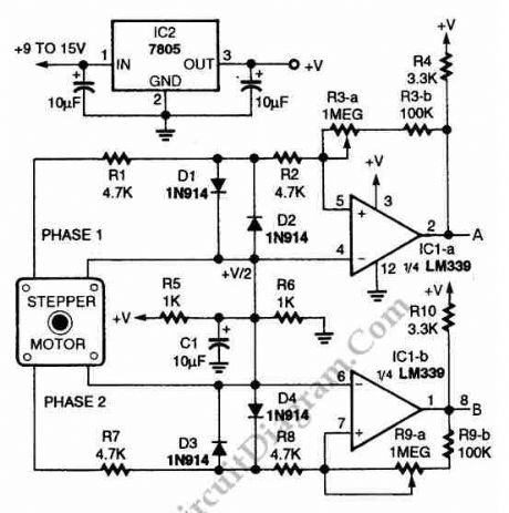
Using circuit depicted in the schematic diagram below, the direction and shaft rotation of stepper motor can be seen on the LED display. Alternative to digital rotation encoder as a digital encoder input, this circuit uses a stepper motor. Here is the schematic diagram of the circuit:
(View)
View full Circuit Diagram | Comments | Reading(3614)
The selectable Voltages 6V, 9V, and 12V Linear Voltage Regulator
Published:2013/3/28 3:55:00 Author:Ecco | Keyword: Selectable Voltages, 6V, 9V, 12V, Linear Voltage Regulator
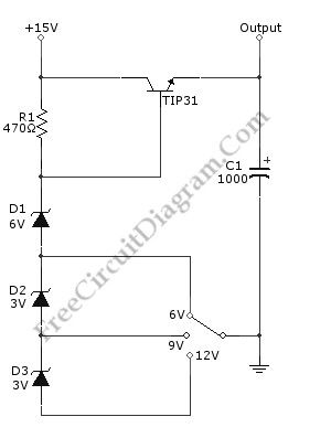
We can build a multiple voltage power supply 6, 9, and 12V (AC-DC Adapter) with the circuit shown in the following schematic diagram. Not only provide multiple voltage output with single voltage supply, this circuit add the benefit of regulating the voltage for better stability. The TIP31 transistor should be installed with proper heat-sink to prevent overheating. A transformer with rectifier diodes and filtering capacitor can be used to supply this circuit. You can use 1 A 15V transformer with 2200uF filtering capacitor for the AC to DC adapter.
(View)
View full Circuit Diagram | Comments | Reading(1399)
Double-Sideband Suppressed-Carrier (DSB-SC) Modulator
Published:2013/3/28 3:50:00 Author:Ecco | Keyword: Double-Sideband Suppressed-Carrier, Modulator

When we modulate a carrier signal with amplitude modulation, there will be four frequency components as the result. The first is the modulating signal itself, the second is the frequency carrier, the the latest two are the difference and the sum of the carrier and the modulating signal. The spectrum of these frequencies can be seen using frequency analyzer. In radio transmission, the modulating frequency components is completely filtered out since the frequency is far lower than the other three. To increase the power efficiency, double sideband suppressed carrier modulator (DSB-SC) remove the carrier frequency part, so the transmitted frequencies consist only the side bands: the sum and the difference. In the schematic diagram below, a double-sideband suppressed-carrier modulator circuit is presented. There is no carrier appear in the output because of the basic current. The Carrier amount appear in at the output can be controlled by adding offsets to the carrier differential pairs. The function of the modulation signal-AM modulation is the amplitude.
(View)
View full Circuit Diagram | Comments | Reading(3362)
The low-Drift High-Impedance JFET DC Voltmeter
Published:2013/3/28 3:49:00 Author:Ecco | Keyword: Low-Drift, High-Impedance, JFET, DC Voltmeter

The voltmeter shown in the schematic diagram below has very high impedance. The range selector uses conventional voltage divider resistors, but since the following pre amplifier uses JFET, the divider can be designed using very high resistance series resistors. This DC voltmeter circuit also featured with low drift. This circuit uses a pair JFETs, which is configured in a balanced-bridge source-follower amplifier circuit. The Q2 and Q1 must be matched within 10% for Idss that will maintains bridge balance over temperature. Here is the schematic diagram of the circuit:
(View)
View full Circuit Diagram | Comments | Reading(2234)
The 60-dB Range Compressor For Audio
Published:2013/3/28 3:48:00 Author:Ecco | Keyword: 60-dB, Range Compressor , Audio
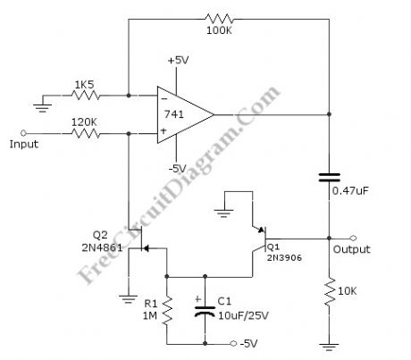
A compressor circuit shown in the schematic diagram below can produce consistent output of 1.4V P-P over entire 60dB range that is very useful for audio level/volume stabilization. As the main components, this circuit uses a 741 opamp and JFET. With input range of 20mV to 2oV, this circuit has delay time of 0.4s (decay time) and response time of 1.2ms (attack time). The JFET is used as voltage-controlled resistor in peak-detecting control loop of 741 opamp. Here is the schematic diagram of the circuit:
(View)
View full Circuit Diagram | Comments | Reading(1092)
5 A Constant Voltage-Constant Current Regulator
Published:2013/3/28 3:44:00 Author:Ecco | Keyword: 5 A, Constant Voltage-Constant Current, Regulator
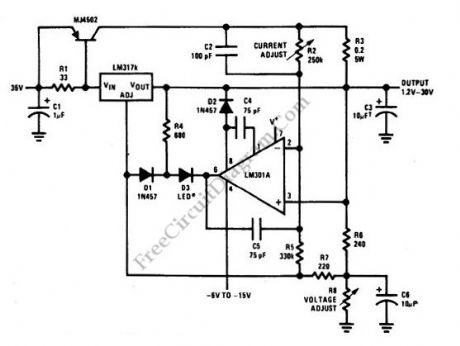
A constant voltage constant current (CVCS) regulator doesn’t mean a system with a constant load, since there will be no regulation in such case. What we call CVCS regulator is a regulator with two modes. The first mode is constant voltage, where the regulator trying to regulate the supply to a variable load at a constant voltage. In this mode off course the current will be variable depending on the load. The current will vary a a range that is limited to a predetermined maximum current level. When the load draw more current than this level then the regulator will switch to constant current mode, where the regulator keep the current at a fixed maximum value. Any attempt of the load to draw more current will cause the regulator to decrease the voltage as a reaction to keep it constant, so it acts like a current limiter. Here is the schematic diagram of the CVCS regulator.
(View)
View full Circuit Diagram | Comments | Reading(1760)
Tremolo Effect Circuit for Electric Guitar or Other Musical Instruments
Published:2013/3/28 3:42:00 Author:Ecco | Keyword: Tremolo Effect , Electric Guitar , Other Musical Instruments
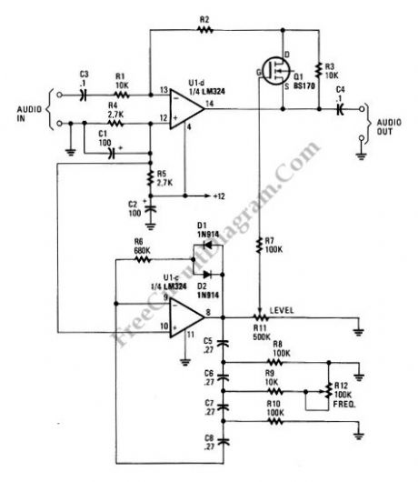
Tremolo circuit is a kind of sound effect. We can see this type of effect is applied in guitar effect pedals. Tremolo effect is produced if we modulate the amplitude of an audio signal. The shape of modulating signal can vary from square wave, sawtooth, or sine. When we use a square wave, then the effect produce a knocking-like sound which might be perceived like a percussive instrument. When we use sine wave then we might perceive a kind of vibrato effect which gives impression that there is a frequency modulation, but it is actually a psycho effect because it modulate only the amplitude, not the frequency. This tremolo circuit use very low frequency (VLF) as a source of modulating signal, with frequency control by R12. The effect’s level, which is modulation depth, is controlled by R11. The amplitude modulation is obtained by controlling the gain of U1D, which has feedback path through Q1 which receives signal from U1C phase oscillator. Here is the schematic diagram of the circuit:
(View)
View full Circuit Diagram | Comments | Reading(2714)
100Hz Wien bridge
Published:2013/3/28 2:00:00 Author:Ecco | Keyword: 100Hz Wien bridge
100Hz Wien bridge is shown as figure.
(View)
View full Circuit Diagram | Comments | Reading(768)
The three-phase bridge rectifier pop n-type filter circuit
Published:2013/3/28 1:47:00 Author:Ecco | Keyword: three-phase, bridge rectifier , pop n-type filter
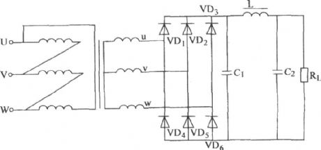
The three-phase bridge rectifier pop n-type filter circuit is shown as figure.
(View)
View full Circuit Diagram | Comments | Reading(1017)
Run/Stop Relay Circuit
Published:2013/3/27 4:22:00 Author:Ecco | Keyword: Run/Stop Relay
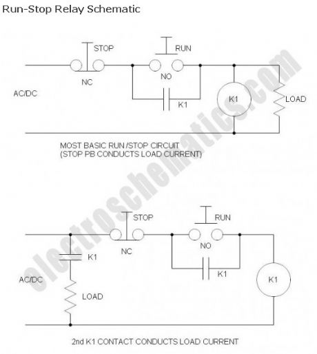
Safety is a major concern in a good many motor-driven applications. This is true in industrial applications where motion starts when power is applied and especially true when power is restored after an outage. In such cases, unwanted or unexpected motion is a risk to life or limb. The most simple solution to this problem is the simple, time-proven Run /Stop Relay Circuit.
With this control circuit, motion cannot commence (or restart) without the operator’s specific pushbutton command. While simple, there are numerous variations and enhancements as you will see, and the benefits are clearly obvious.
(View)
View full Circuit Diagram | Comments | Reading(1143)
| Pages:44/471 At 204142434445464748495051525354555657585960Under 20 |
Circuit Categories
power supply circuit
Amplifier Circuit
Basic Circuit
LED and Light Circuit
Sensor Circuit
Signal Processing
Electrical Equipment Circuit
Control Circuit
Remote Control Circuit
A/D-D/A Converter Circuit
Audio Circuit
Measuring and Test Circuit
Communication Circuit
Computer-Related Circuit
555 Circuit
Automotive Circuit
Repairing Circuit