
Index 5
1KHz Square Wave Generator Circuits
Published:2013/11/10 20:08:00 Author:lynne | Keyword: Square Wave Generator
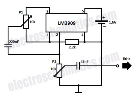
You can build a simple 1KHz square wave generator using a few components and the LM3909 that is useful for testing audio equipment. It is powered from a single 1.5V battery cell and the maximum amplitude of the output signal is 1.1V. With P1 you can adjust the symmetry of the square wave signal and with P2 the amplitude.Square wave generator schematic
(View)
View full Circuit Diagram | Comments | Reading(1039)
Automatic Solar Garden Lights with LEDs Circuit
Published:2013/11/10 20:04:00 Author:lynne | Keyword: Automatic Solar Garden Light
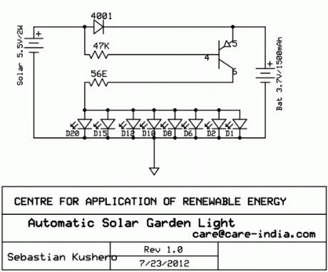
Efficient automatic solar garder lights circuit with minimum components the best deal is that is completely auto and the Solar panel acts as a light detector. Switches the Lamp off at Dawn, charges the battery during daytime and switches the LED lights ON at dusk providing 100 Lumens illumination during the night.
The solar panel must provide 5.5V and 150mA. Assuming a 3.7V/1500mAh battery the charging will be complete in 8 hours at 200% capacity @ 180 mA. With 10 LEDs the power consumption would be 90 mA/hour providing a 10 hours illumination with light levels of 50 lumens to 60 lumens. With 20 LEDs the light intensity will be 100 to 120 lumens.
You can use any number of LEDs and battery capacity too. This would directly provide you the amount of illumination and time for illumination. If youusehighercapacitybatterythanthatrecommended thesolarpanelcurrentshouldbeincreasedproportionately. Current provided by solar panel should be 10% of battery capacity.
Solar garden lights circuit schematic
Bill of material for the solar garden lights
Resistor(1)4K7or5K6
Resistor(1)47Eor56Eoranyvalue(CurrentLimiting)
Transistor2N3906
Diode1N4001/7/1N4148(Any)
SolarPanel5.5v/200mA
Battery3.7v/1500mAh
SwitchSPST (View)
View full Circuit Diagram | Comments | Reading(1719)
Light Activated Switch Circuit
Published:2013/11/6 19:17:00 Author:lynne | Keyword: Light Activated Switch Circuit
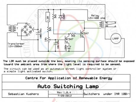
The light activated switch circuit can be used for switching OFF a particular lamp or group of lamps in response to the varying ambient light levels.The unit once built can be used for switching OFF a lamp when dawn breaks and switching it ON when dusk sets in.The power supply is a standard transformer, bridge, capacitor network, which supplies a clean DC to the circuit for executing the proposed actions.
Automatic light activated switch circuit schematic
The LDR must be placed outside the box, meaning its sensing surface should be exposed toward the ambient area from where the light level is required to be sensed. The circuit can be used as an automatic street light controller system or a simple light activated switch. (View)
View full Circuit Diagram | Comments | Reading(1223)
Pathway Lighting with LEDs Circuit
Published:2013/11/6 19:15:00 Author:lynne | Keyword: Pathway Lighting
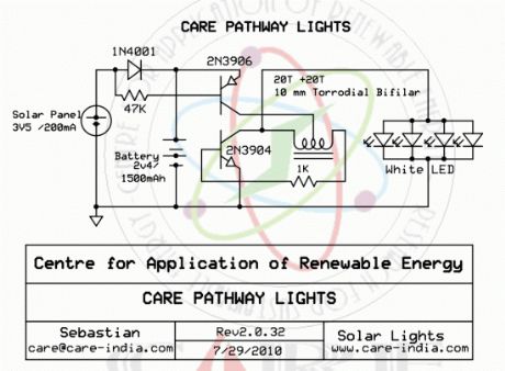
Simple pathway lighting that would provide illumination for the path at night. Extension for the Solar garden Light. The torroid is bifilar wound. The Torroid is 10mm and Cat 5 cable is wound around the same.Solar panels of 3.5 maybe difficult to procure using 2 2V panels in series could be used. If you do use 4V panel then suggest you add another diode in series with 1N4001 to drop voltage to contain voltage to the battery.
The characteristic voltage for a white LED is 3.2V but the addition of the torroid provides the boost to drive the white LED. If you cannot procure the battery as suggested you can use 600 mAH battery then do not go above 3/4 LED’s.
Pathway LED Lights Schematic
(View)
View full Circuit Diagram | Comments | Reading(1294)
Firefly Lights
Published:2013/11/6 19:07:00 Author:lynne | Keyword: Firefly Light
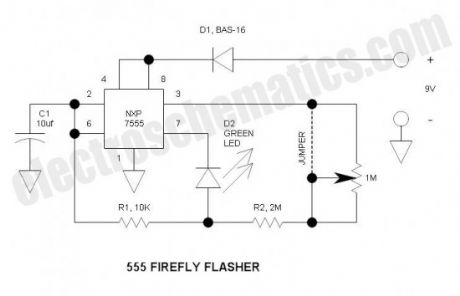
This firefly lights flasher is an easy, fun project. It can be built on the tiny circuit board, or on perf board.
Specifications
Battery life: approx 1 year using the NXP 7555 CMOS timer IC & standard alkaline battery, or about 6 months using the more common TI TLC555
Flash rate: approx 0.25 Hz (unless using optional potentiometer)
Dimensions: 14.5mm2
Minimum voltage: approx 6V
Schematic of the Firefly Flasher Circuit
Bill of Materials (if on perf board, use standard through-hole rather than SMT components)
PCB ExpressPCB.com
U1 NXP 7555 or TI TLC555 Timer IC, SOIC-8
R1 10K, 0805
R2 2M, 0805
R3 Potentiometer, 1M , 0.2” lead spacing (optional)
C1 10uF, 25V, X7R, Ceramic, 0805
D1 Diode, BAS16, or MMBD4148, SO23-3
D2 LED, Green, High Brightness, 0805
Battery Standard 9V
How the firefly lights works
It functions like almost any 555 astable timer, except that the LED is inserted into the capacitor reset path so that when pin 7 discharges C1 to common, this relatively high current must pass through the LED. In this way, the average battery current is only about 100µA. When battery voltage becomes very low, the LED threshold voltage prevents discharging C1 down to the lower threshold – when this happens, R2 finishes off the discharge because the output switches to ground potential the same time pin 7 turns on – you will find that this works on almost dead batteries that may be useless for other applications. D1 protects against accidental reverse battery voltage.
Background
Fireflies are common through Northeastern US and also in many other parts of the world. This green LED has the same color, flashes at about the same duration and has a similar repetition rate just like a real firefly (lightning bug). Put a number or these around your grounds and they will truly resemble fireflies – there will be no synchronization of the flashes. The only thing this cannot do is to fly – fireflies ascend as they flash, and they do not flash when perched to protect from predators. Also, this is much larger than the tiny firefly beetle that measures about 3 x 20mm.
(View)
View full Circuit Diagram | Comments | Reading(1091)
12V LDO Solar Charge Controller
Published:2013/11/5 19:11:00 Author:lynne | Keyword: LDO Solar Charge Controller
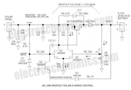
This Low Dropout Voltage (LDO) solar charge controller uses a simple differential amplifier and series P channel MOSFET linear regulator—their compatibility seems like a marriage made in heaven. Voltage output is adjustable. It is mainly intended for charging 12V lead-acid batteries.
Solar Charge Controller Specifications
Solar panel rating: 50W (4A, 12V nominal) (open circuit voltage: 18 to 20V)
Output voltage range: 7 to 14V (adjustable) (not recommended for 6V applications)
Max power dissipation: 16W (includes power dissipation of D3)
Typical dropout voltage: 1.25V @ 4A
Maximum current: 4A (current limiting provided by solar panel characteristics)
Voltage regulation: 10mV (no load to full load)
Battery discharge: 1mA (Chinese controls discharge at typically 5mA)
LED indicators:
RED: Solar panel active
GREEN: Series regulator limiting current (fully charged or topping off)
Reverse battery protection: Control shuts down if battery is inadvertently connected reverse
12V Solar Charge Controller Schematic
Bill of Materials
In Excel format (download link at the bottom)
Dropout Voltage
The input voltage exceeds the input voltage by 1.25V when charging at the maximum rate—the lower, the better. Low Dropout Voltage (LDO) is the catch phrase for anything under approximately 2V. This could potentially be reduced to below 1V by making D3 a schottky rectifier.
Current Limiting
Current limiting is provided by the solar panel—it is not a commonly understood fact that the solar panel tends to be a constant current device. For this reason, a solar panel can withstand a short circuit. Therefore, the control does not need current limiting.
Float Charge of Lead-Acid Batteries
This control charges the battery at a constant voltage and also maintains a charged battery (float charge). The float charge voltage specification is a little lower than the charge voltage, so to accommodate both voltages, a compromise is reached by simply reducing the voltage slightly—that is how ALL automotive systems operate. To obtain maximum charge in a 12V battery, set the control to 14 to 14.6V. Automotive systems further reduce voltage to 13 to 13.5V in order to accommodate high temperature operation as the battery is usually located in the hot engine compartment—battery has a negative thermal coefficient of voltage.
Voltage Adjustment
To set the voltage, disconnect the battery and connect a 1K dummy load resistor to the output. The resistor is necessary to shunt potential MOSFET leakage current as well as the green LED current.
LDO Solar Charge Control Circuit Operation
R4 and D1 form a 6V shunt zener voltage reference. Q1 & Q2 make up the classic differential amplifier that amplifies the difference between the reference voltage and the feedback voltage from the arm of potentiometer R6. The output is taken from the collector of Q1 and drives the gate of P Channel MOSFET Q3. Differential voltage gain is probably in the order of 100 to 200. For best performance, I selected Q1 & Q2 for matched hFE. As the feedback voltage increases at the arm of R6, Q2 turns on harder and steals some of the emitter current away from Q1. The collector current of Q1 follows the emitter current and drops less voltage across R1 thus reducing Vgs of Q3 and turning it off. C2 provides frequency compensation to prevent the amplifier from oscillating.
Q3 is dormant unless the battery is connected reverse—should this happen, Q3 turns on and reduces the reference voltage input to zero thus turning Q1 & Q3 and preventing damaging battery current.
D3 prevents the battery voltage from appearing across an inactive solar panel.
Thermal Management
This is a linear series regulator that dissipates significant power when the pass transistor is both conducting current and dropping voltage simultaneously—during maximum charge rate when the voltage drop is low, the heatsink runs warm—when the battery is fully charged and there is low charge current, the heatsink is cold—but when the battery starts to top off at maximum voltage, the heatsink runs very hot—such is the nature of a linear regulator. At 4A, Q3 drops 3.3V (assuming solar panel voltage is 18V)(the remaining 0.7V is the D3 voltage drop. P = 4A * 3.3V = 13.2W. The heatsink is rated at 3.9°C/W, so heatsink temperature rise = 13.2W * 3.9°C/W = 51.5°C. Adding the 25°C ambient temperature results in a heatsink temperature of 76.5°C. While this may seem very HOT to the touch, it is still cool to the transistor that is rated for a junction temperature of 175°C.
For the Future
A 6V version—while this control may be adjusted down to 7V for charging 6V batteries, the performance is marginal, but will function at reduced current. A 6V version is on the drawing board.
Photo
Perf board—sorry, no circuit board artwork at the time of publication. (View)
View full Circuit Diagram | Comments | Reading(1515)
Security Light & Switch with PIR Sensor Update Circuit
Published:2013/11/5 19:09:00 Author:lynne | Keyword: Security Light, Switch
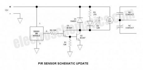
This is a simple update to Mr. Hareendran’s PIR Sensor Security Light circuit. It has a shortcoming limits the relay voltage to approximately 3.3V. While this may function with some 5V relays, it will not function with all. The nature of an emitter follower Darlington forces the output voltage to be two junction drops below the base drive voltage plus a small voltage drop across R1.
In keeping with the spirit of his design, I retained the Darlington arrangement, and the transistor type number – however, I changed the transistors from common collector to common emitter configuration, and connected the relay between the collector output and the positive rail. The relay now utilizes a 12V coil – to use an existing 5V relay, simply add a resistor in series with the coil whose value is scaled up from the coil resistance. Also, I connected the LED across the relay coil rather than powering it via the 2nd relay contact – this way, only one form “C” relay contact is required thus making the relay less expensive – of course it can be done either way. I eliminated some additional, unneeded components.
Security Switch & Light Circuit Schematic
How it works
When motion is detected, the output (pin 2) goes to 5V and current flows through R2 to the base of Q1. The emitter current of Q1 becomes the base current of Q2 – the current gain of a Darlington is the hFE squared or about 10,000 to 50,000 (very high). This easily provides adequate drive current for the relay. R1 provides a means of conducting any potential leakage in Q1 to common and also helps Q2 to turn off faster. D1 is the back diode that circulates the relay coil current when Q1 & Q2 turns off thus preventing a damaging voltage transient.
Testing
No, I did not build and test this one – I just happen to know from experience that this circuit will work OK – if the circuit was new to me, I would definitely Protoboard and test because Murphy may be lurking somewhere. Murphy’s Law states that anything that can go wrong will go wrong… Such is true as I have proven it numerous times.
For the Future
PIR crystal amplifier circuit – yes, it is not difficult.
(View)
View full Circuit Diagram | Comments | Reading(1219)
6V LDO Solar Charge Controller
Published:2013/11/4 20:18:00 Author:lynne | Keyword: LDO Solar Charge Controller
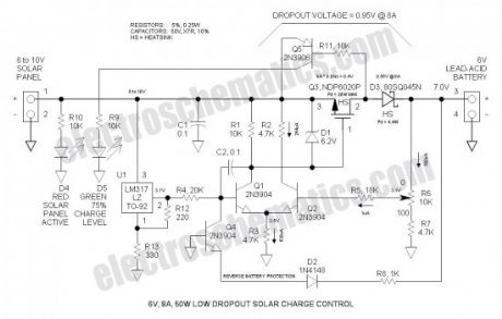
This Low Dropout Voltage (LDO) solar charge controller is a variation of the previously posted 12V LDO controller. It is optimized for charging a 6V lead-acid battery with a 9V solar panel. Minimum voltage drop is less than 1V. It uses a simple differential amplifier and series P channel MOSFET linear regulator. Voltage output is adjustable. It may also be applied in two or four cell lead-acid applications (4V & 8V).It is not recommended for 12V applications.
6 Volt solar charge controller schematic
6V Solar Charge Controller Specifications
Max solar panel rating: 50W (8A, 6V nominal) (open circuit voltage: 9 to 10V)
Output voltage range: 4.7 to 9.8V (adjustable) (not recommended for 12V applications)
Max power dissipation: 16W (includes power dissipation of D3)
Typical dropout voltage: 0.9V @ 8A (less @ lower currents)
Maximum current: 8A (current limiting provided by solar panel characteristics)
Voltage regulation: 80mV (no load to full load)
Battery discharge: 1mA (Chinese controls discharge at typically 5mA)
LED indicators:
RED: Solar panel active
GREEN: Series regulator limiting current (fully charged or topping off)
Reverse battery protection: Control shuts down if battery is inadvertently connected reverse
Operation at lower current/power
While designed for 8A, 50W, it will function just as well at much lower current /power.
LDO Solar Charge Control Photos
Perf board—sorry, no circuit board artwork at the time of publication. (View)
View full Circuit Diagram | Comments | Reading(2416)
AC/DC Microammeter Circuit
Published:2013/11/4 20:16:00 Author:lynne | Keyword: AC/DC Microammeter Circuit
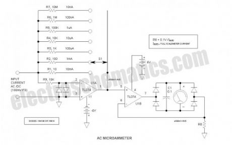
This is a take-off on Mr. Marian’s “Simple Micro Ampere Meter Circuit” that utilizes active circuitry and an analog meter to make sensitive DC current measurements. A reader subsequently asked if it could measure AC microamperes and that is what spawned the idea.
While the schematic is similar, there are notable differences—the voltage drop is now 100mV rather than 1V, the sensitivity is 10nA full scale rather than 100nA and it now measures AC or DC. A precision rectifier rectifies the AC voltage so that a DC meter may be used.
Microammeter Circuit Schematic
(View)
View full Circuit Diagram | Comments | Reading(3603)
MODEL RAILWAY TIME
Published:2013/11/3 20:36:00 Author:lynne | Keyword: MODEL RAILWAY TIME
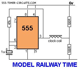
Here is a circuit that will convert any clock mechanism into Model Railway Time. For those who enjoy model railways, the ultimate is to have a fast clock to match the scale of the layout. This circuit will appear to make time fly by turning the seconds hand once every 6 seconds. The timing can be adjusted by changing the 47k. The electronics in the clock is disconnected from the coil and the circuit drives the coil directly. The circuit takes a lot more current than the original clock (1,000 times more) but this is one way to do the job without a sophisticated chip. (View)
View full Circuit Diagram | Comments | Reading(1055)
Engine Running Detector, Load Switch
Published:2013/10/29 20:40:00 Author:lynne | Keyword: Engine Running Detector, Load Switch
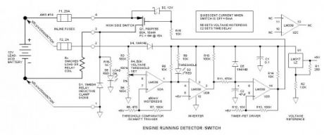
This circuit determines when an engine is running, and when running, it turns on a solid-state switch to automatically power accessories. It does this simply by measuring battery voltage—when not charging, battery voltage is less than approx. 13.2V—when charging, it is greater than approx. 14.0V. Seems like a simple task, does it not? If so, why are there not already devices available to do this seemingly simple task?
While the concept is simple, there are numerous problems involved as follows:
Voltage must be sensed as close to the battery as possible, and voltage sense wiring must be separate from power wiring—hence the requirement for the Kelvin connection. This is why I wrote the recent article:What is a Kelvin Connection?
Since this circuit is connected directly to the battery, circuit protection is absolutely essential. This is why I wrote the recent article:Low Voltage & Automotive Circuit Protection.
Voltage threshold must be accurate—requires stable voltage reference.
Circuit must have hysteresis for positive switching.
Load switch must have substantial delay to prevent unintended or nuisance switching.
Quiescent current must be low to prevent battery discharge.
Charging system must function correctly—alternator must float charge the battery as well as power all connected accessories when engine is at idle speed.
Due to variations in battery charging voltage in different systems and a relatively narrow voltage threshold window, there is no one size fits all voltage setting. As a result, the threshold must be adjustable.
Due to these complexities, this circuit is not recommended for the novice. However, if installed using proper circuit protection & wiring practices, the only failure mode is unintended battery discharge should it not automatically disconnect the load.
(View)
View full Circuit Diagram | Comments | Reading(1522)
STEPPER MOTOR CONTROLLER Circuit
Published:2013/10/27 21:14:00 Author:lynne | Keyword: STEPPER MOTOR CONTROLLER
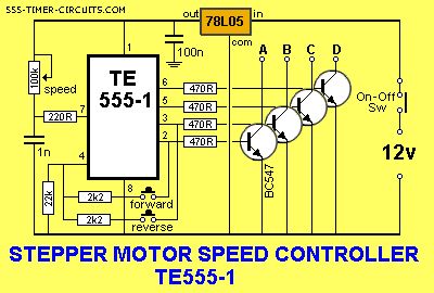
The direction of rotation is determined by the FORWARD and REVERSE switches and the motor does not take any current when a switch is not pressed. (View)
View full Circuit Diagram | Comments | Reading(1782)
REACTION TIMER GAME Circuit
Published:2013/10/27 21:10:00 Author:lynne | Keyword: REACTION TIMER

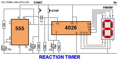
This is a game for two players. Player 1 presses the START button. This resets the 4026 counter chip and starts the 555 oscillator. The 555 produces 10 pulses per second and these are counted by the 4026 chip and displayed on the 7-Segment display. The second player is required to press the STOP button. This freezes the display by activating the Clock Inhibit line of the 4026 (pin 2).Two time-delay circuits are included. The first activates the 555 by charging a 10u electrolytic and at the same time delivering a (high) pulse to the 4026 chip to reset it. The second timer freezes the count on the display (by raising the voltage on pin 2) so it can be read.
(View)
View full Circuit Diagram | Comments | Reading(1400)
555 (TLC555) Relay Driver Circuit
Published:2013/10/21 20:33:00 Author:lynne | Keyword: Relay Driver Circuit
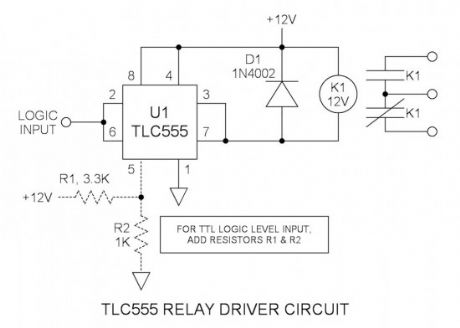
Many integrated circuits have undocumented features or abilities. This is one of them. The TLC555 output (pin 3) can sink a 100mA load to 1.28V. The open drain transistor reset (pin 7) can sink 100mA to 1V. Tying both lines together is permissible because they are logically the same polarity and this potentially doubles the sink current ability to 200mA. This is ideal for driving my 133mA relay coil.The input also has the undocumented, but better known, feature of a Schmitt trigger that provides positive switching.
555 Relay Driver Schematic
Output current rating (pin 3): TLC555 vs. NE555
(Vcc = 15V)
TLC555
NE555
Source current
10mA
200mA
Source mode saturation voltage
Vcc-0.8V
Vcc-2.5V
Sink current
100mA
200mA
Sink mode saturation voltage
1.28V
2.5V
While it can be seen that the NE555 has the higher current rating, its saturation voltage is grossly inferior and this is a detriment in driving loads without excessive voltage drop. Also it can be seen that the TLC555 is much like TTL in that its sourcing ability is far less than its sinking ability. However for driving a relay, we are interested only in current sinking properties. (View)
View full Circuit Diagram | Comments | Reading(1486)
Inverted 555 Timer Circuit
Published:2013/10/17 20:26:00 Author:lynne | Keyword: Inverted 555 Timer Circuit
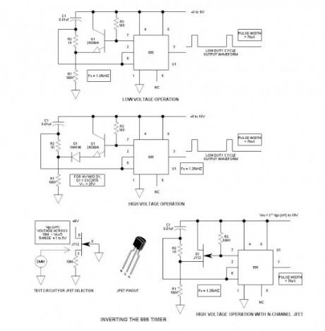
Whenever I use the 555 timer, it seems that the output polarity is invariably incorrect, and the way the 555 functions, it normally cannot generate a duty cycle of less than 50% — 90% yes, 10% NO! This inverted 555 circuit generates duty cycles of less than 50%. Everything works the same except for the polarity. Why not simply invert the output with a transistor? Will not that do the same? Legitimate question… Actually NO, because a transistor that inverts the output cannot provide the desirable totem pole source/sink output function of pin 3. And there is another reason that we will get in the future—this is a 555VCO circuit that requires the inverted timer.
Inverted 555 Timer Schematic
The schematic shows (3) circuits, because one circuit does not work well over the entire Vcc range.
The first simply uses a “normal” 2N3904 garden variety transistor, and this works well when Vcc < 9V. When Vcc > 9V, the base to emitter junction starts to zener and disrupts operation. Transistor base to emitter junction zeners a little above -6V.
The second circuit adds D1 to the emitter of Q1 in order to increase VEBO. With this mod, Vcc may be increased to the 18V limit. However, D1 may be eliminated if we use the special 2SC2878 switching transistor that has a VBEO rating of -25V. These devices are no longer in production, but are available on eBay—every serious experimenter should have a few in his component collection. The types now in production use the tiny SO-23 SMD package.
The third circuit uses a J112 N-Channel JFET for Q1. The JFET is a curious device that works well for the application provided we allow for the VGS(OFF) parameter. VGS must be less than Vcc /3. (e.g. if Vcc = 9V, VGS(OFF) must be less than 9V /3 or 3V for proper operation). Since the VGS(OFF) parameter is sloppy (-1 to -5V), the device must be selected—to the left is a simple test circuit—actually, most devices will work OK. The J112 should also be in every serious experimenter’s component collection. (View)
View full Circuit Diagram | Comments | Reading(1204)
Relay Driver Circuit 2
Published:2013/10/16 20:20:00 Author:lynne | Keyword: Relay Driver Circuit 2
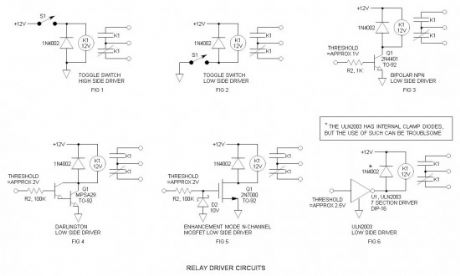
Relays have been around for a long time and though often now replaced with solid state switches, they have unique properties that make them more robust than solid-state devices and are not going away. The unique properties are high current capacity, ability to withstand ESD and drive circuit isolation.
There are numerous ways to drive relays. In preparation for some of the more advanced relay drivers I will be posting in the future, I have listed a few basic relay drivers for your reference. Included are the following: High side toggle switch driver, low side toggle switch driver, bipolar NPN transistor driver, Darlington transistor driver, N-Channel MOSFET driver, and ULN2003 driver.
Relay Driver Schematic
Advantages of the low side driver
Easy to interface to low voltage logic circuitry
Far more interface options including the popular ULN2003 driver
Fewer components
Uses more commonly available and less expensive NPN drive transistors
Relay power may be sourced by a higher, unregulated voltage—reduces load on voltage regulator
Easier to interface relay economy feature—will be discussing this in the future
Industry standard technique
Relay driver, how it works?
Generally, we think on the high side because we usually place the power switch in the power lead as in Fig 1. The same may be accomplished by locating the switch in the low side or return lead as in Fig 2. When controlling relays via logic etc. it is far easier to interface to the low-side driver. For low power relays, a 2N4401 is a good choice (Fig 3). If you desire to drive a larger relay or want less base current, a Darlington driver (Fig 4) is recommended. If driving via CMOS logic, an enhancement mode MOSFET is a good choice (Fig 5). If you nave a number of relays or other loads to drive (like a 7 segment LED display), the ULN2003 is a great choice. (Fig 6).
Clamp diode
The clamp, free-wheeling or commutation diode provides a path for the inductive discharge current to flow when the driver switch is opened. If not provided, it will generate an arc in the switch—while the arc will not generally damage a switch contact, it will cause contact degradation over time—and yes, it will destroy transistors—been there, done that. The diode requirements are non-critical and a 1N4148 signal diode will generally work OK in low power applications.
The ULN2003 has internal clamp diodes. While these work OK in non-critical applications, I have had problems with them generating “glitches” in supposedly unrelated sections.
Avoid emitter follower drivers
I have not included an example of this because I do not wish to promote this technique. This is a high-side driver accomplished by an emitter follower transistor. They are frequently found on electroschematics.com, but they are not the driver of choice for three reasons as follows:
It turns the relay itself into a voltage threshold detection device—while it may work, it was not designed for this function and the threshold may vary greatly from device to device.
The emitter follower transistor requires a base drive voltage that should go essentially to the positive rail or the relay may not pick up. Only relays that have a low pick-up voltage work OK.
The voltage hysteresis is extreme—once turned on, it is often difficult to turn off again.
For the future
Relay economy driver circuits
Voltage doubler relay driver
Glossary of undocumented words and idioms (for our ESL friends)
glitch –undesirable noise transient or spike (in electronics)
(View)
View full Circuit Diagram | Comments | Reading(1551)
LDR Pole Light Switch
Published:2013/10/13 20:38:00 Author:lynne | Keyword: LDR Pole Light Switch
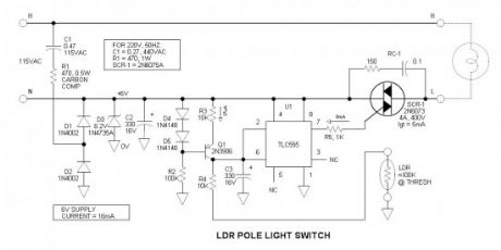
My vintage (62 year old) pole light has always been controlled by a timer—a source of continual frustration due the requirement of readjustment for the ever-changing seasons. However, after knocking it over (I backed my car into it…), I decided it was time for an update. The circuit consists of a light dependent resistor (LDR), TLC555 (applied as Schmitt trigger), and a TRIAC power switch. The complete assembly neatly fits inside the steel pole light tube and the LDR peeks out through a hole in the side. This was really a fun project, and useful to boot.
Pole Light Switch Circuit Schematic
Power supply
The power supply is the typical capacitor limited charge pump type that is zener regulated at 6.2V. Due to the lack of isolation, I was careful to identify the return conductor so that the electronics (including the LDR) would not be floating on the hot lead. For safety, most of the testing was done using an isolation transformer. R1 must absorb a high peak power transient current when power is applied, so a carbon comp, ceramic comp, or wire wound resistor is recommended. Maximum DC current available is 16mA. Actual load is about 6mA. My application was 115V, 60hZ. For 230VAC, the components are indicated on the schematic. In this circuit, +6V is the power return lead, and 0V is the electronic circuit common—to visualize this, one must screw his head on backwards…
LDR
The light dependent resistor (CdS photocell) that I used was in the TO-5 package that is well adapted for poking through a hole and is held in place with silicone rubber. The Clairex CL703M19 LDR that I used is no longer available and I have been unable to locate the specs. The DigiKey PDV-P8103-ND appears to be a reasonable choice, but may require bias current tweaking to set the threshold.
555 Schmitt trigger driver
A TLC 555 was used as a voltage threshold detecting device with hysteresis. Pin 7 drives the TRIAC gate directly via its open collector output. This is a rather unconventional application. The CMOS version is used to minimize power supply load—I tried a bipolar 555 and it worked, but the power supply ripple voltage doubled to about 0.5VP-P.
Constant current bias—Threshold adjustment
Because the 555 has so much hysteresis, I feared that the ON & OFF thresholds would be too far apart. To help reduce the hysteresis, the LDR is biased by a current source. Q1 is wired as a current source—its collector current does not vary with collector voltage. This technique essentially increases the “gain” of the LDR. The current is set via adjusting the emitter resistor (R3)—it drops about 0.37V.
C3 makes the circuit insensitive to rapid changes in light intensity. It takes about 60sec to turn on.
Logic TRIAC
The logic TRIAC is an interesting device. It can be triggered by either a positive or negative gate current regardless of voltage blocking polarity. For maximum sensitivity, I used negative gate current. The device I used had an actual Igt (gate current sensitivity) of 1.5mA that is well below the 5mA Max specification. However, gate overdrive (5mA in my case) is recommended to assure that it fires at low winter temperatures. Quencharc RC-1 is connected across the TRIAC to help control turn-off voltage transients.
Choice of lighting
For the time being, I am sticking with the vintage incandescent lamp—it is a matter of aesthetics. I will upgrade to LED technology only when its color balance matches incandescent. (View)
View full Circuit Diagram | Comments | Reading(1130)
Relay Economy Circuit
Published:2013/10/10 20:12:00 Author:lynne | Keyword: Relay Economy Circuit
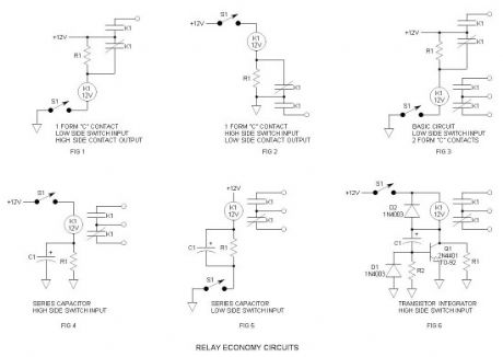
Relays continue to be useful and popular, but in low-power, battery operated applications they tend to be power wasters. The following relay economy circuits reduce coil power significantly by simply adding a series resistor. As soon as the relay picks up, the coil voltage is reduced either by the normally closed contact opening or the charging of a capacitor that is connected in parallel with the economy resistor. Included is the standard relay economy circuit as well as two additional circuits that may be new to the world.
Note that these relay economy circuits may be used in conjunction with the relay driver circuits previously posted: www.electroschematics.com/7123/relay-driver-2/
Figures 1 & 2 show how high and low side drivers can be connected to provide relay economy. The unused normally open relay contact provides the output. If an isolated contact is required, a two pole relay must be used as in figure 3.
Figures 4 & 5 solve the problem by simply adding a capacitor in parallel with the resistor. This allows the use of a single pole relay. The required capacitance is high, but voltage is low so that the size is physically manageable.
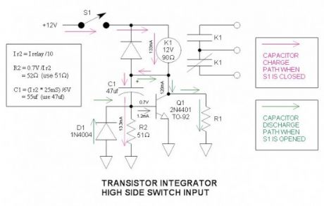
Figure 6 shows how to reduce the capacitor size by a factor of 20 by use of a simple transistor integrator. The collector voltage of Q1 integrates to the maximum voltage allowed by R1 in about 25mS.
Red arrows indicate capacitor charge pathGreen arrows indicate capacitor discharge pathC1 integrates slowly due to the limited current flowing through R2. The voltage across R2 is limited by the Vbe of Q1 (0.7V) while integrating. (View)
View full Circuit Diagram | Comments | Reading(1104)
Bicycle Anti-Theft Alarm Circuit
Published:2013/10/10 20:09:00 Author:lynne | Keyword: Bicycle Anti-Theft Alarm Circuitv
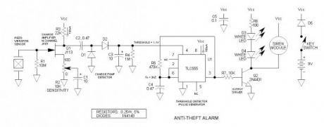
I hate to suggest the specific application ‘bicycle’ because it may be use to protect many items from theft. This anti-theft alarm project is built around the inexpensive Measurement Specialties DT piezo film sensor. Every now and then everything seems to work out perfectly as in the Yin and Yang of the cosmos, and this is one of them.It is simple, inexpensive and practical… (View)
View full Circuit Diagram | Comments | Reading(999)
Automatic Door Light Switch
Published:2013/9/28 21:08:00 Author:lynne | Keyword: Automatic Door Light Switch
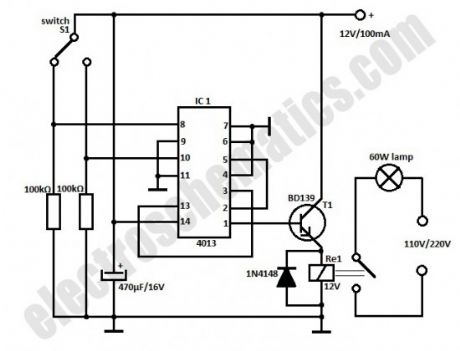
This automatic door light switch circuit turns ON a lamp when a door is opened then turns it OFF when the door is opened again. The working principle of the light switch is quite simple. The bistables inside CMOS 4013 are conected in series. FF2 is configured as a R-S memory to store the state of the switch. S1 must switch as soon as the door opens that is why it will be mounted on the door jamb.
When the door will be opened FF2 is registered and its output (pin 13) will be 1.This output, connected at the tact entry of FF1 (pin 3) will open T1 and activate the relay switching ON the light.
When the door is closed nothing will happen because FF2 is unregistered and its output (pin 13) passes in state “0″. Only when the door is opened again, FF1 will change its state and the output at pin 1 will block the transistor so the relay will be disconnected and the door light switch turns off the lamp.The relay must operate at voltages between 5 V and 15 V.
(View)
View full Circuit Diagram | Comments | Reading(1611)
| Pages:5/312 1234567891011121314151617181920Under 20 |
Circuit Categories
power supply circuit
Amplifier Circuit
Basic Circuit
LED and Light Circuit
Sensor Circuit
Signal Processing
Electrical Equipment Circuit
Control Circuit
Remote Control Circuit
A/D-D/A Converter Circuit
Audio Circuit
Measuring and Test Circuit
Communication Circuit
Computer-Related Circuit
555 Circuit
Automotive Circuit
Repairing Circuit