
Switching-Regulator Circuit
Index 7
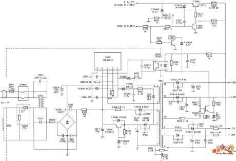
STR40090 series switching power supply thick film circuit diagram
Published:2011/4/11 4:12:00 Author:Nicole | Keyword: switching power supply thick
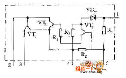
View full Circuit Diagram | Comments | Reading(1424)
Simple and practical switching power supply circuit diagram
Published:2011/4/2 3:40:00 Author:Rebekka | Keyword: switching power supply
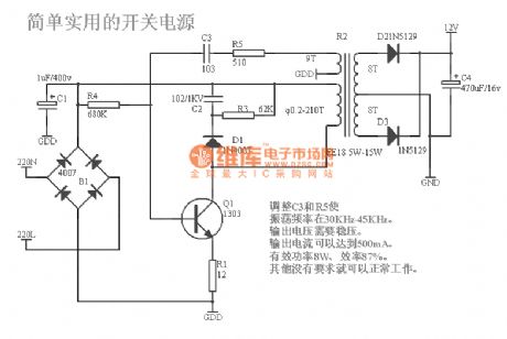
Simple and practical switching power supply circuit diagram is shown as below. Adjust C3 and R5 to keep the vibration frequency between 30KHz~45KHz. The output voltage should be steady voltage. Output current can up to 500mA. Effective power 8W, 87% efficiency. It can work if you don't have other requirement.
(View)
View full Circuit Diagram | Comments | Reading(6785)
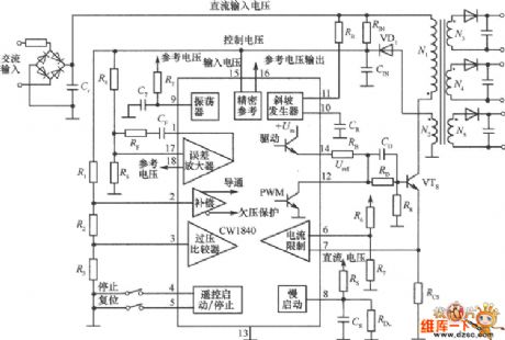
Composed of CW1524 buck chopper switching regulator circuit diagram
Published:2011/4/1 3:26:00 Author:Rebekka | Keyword: buck chopper switching regulator
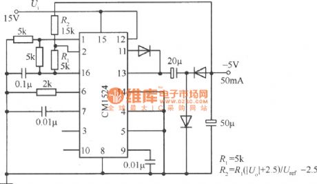
Composed of CW1524 buck chopper switching regulator circuit diagram is shown as below.
(View)
View full Circuit Diagram | Comments | Reading(921)
Composed of MC33364 8.2V/3A switching DC regulator power supply circuit diagram
Published:2011/4/1 3:27:00 Author:Rebekka | Keyword: switching DC regulator
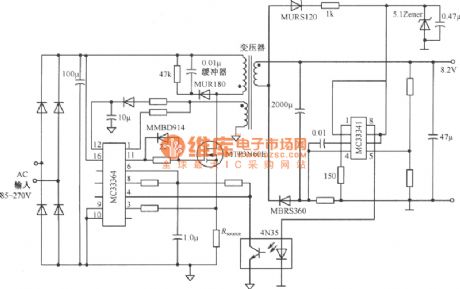
Composed of MC33364 8.2V/3A switching DC regulator power supply circuit diagramis shown as below.
(View)
View full Circuit Diagram | Comments | Reading(1437)
Composed of MC33363 6V/2A isolated switching regulator power supply circuit diagram
Published:2011/4/1 3:29:00 Author:Rebekka | Keyword: isolated switching regulator
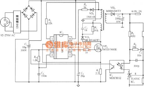
Composed of MC33363 6V/2A isolated switching regulator power supply circuit diagramis shown as below.
(View)
View full Circuit Diagram | Comments | Reading(3697)
Composed of CS3843 and CS5101 output 5V/3.3V switching DC power supply circuit diagram
Published:2011/4/1 3:21:00 Author:Rebekka | Keyword: switching DC , power supply
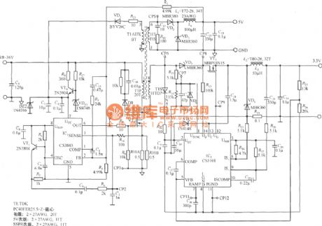
Composed of CS3843 and CS5101 output 5V/3.3V switching DC power supply circuit diagram is shown as below. CS3843 is a fixed frequency PWM controller. The IC is characterized by setting a tone oscillator that used to precisely control duty cycle. There are a reference voltage after temperature compensation, a high-gain error amplifier, current sense comparator and a high current push-pull output that suitable for driving the power tube MOSFET. CS5101 is a bipolar secondary side of the end of class regulator and regulation accuracy can up to 1.0%. Gate drive voltage is 8.0~75V, operating voltage(Ucc) is 8.0~45V, peak output current is 1.5A. There are one 2.0% accuracy, precision voltage reference and an internal compensation error amplifier.
(View)
View full Circuit Diagram | Comments | Reading(1870)
LM2622 adopted triple output switch power supply circuit diagram
Published:2011/4/1 3:16:00 Author:Rebekka | Keyword: triple output switch
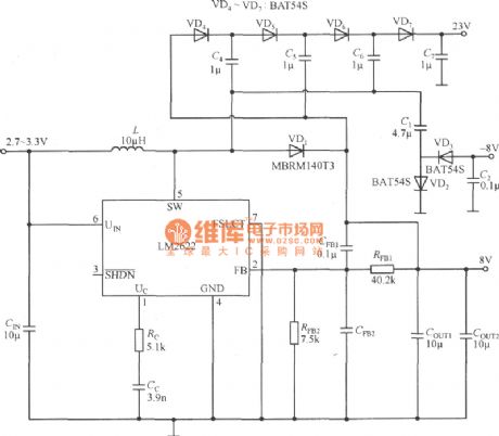
The power circuit diagram of triple output switch posed by the LM2622 is shown as below. LM2622 is a 600kHz step-up PWM DC / DC Converter. It converts 3.3V input voltage to8V, -8V and 23V three output voltages. The output current can up to l.6A. You can use filters and low noise components, the voltage can be as low as 2.0V.
(View)
View full Circuit Diagram | Comments | Reading(1768)
Composed of MAX1822 and MAX333 1~4 channel load switch circuit diagram
Published:2011/4/1 3:14:00 Author:Rebekka | Keyword: 1~4 channel load switch
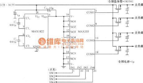
Composed of MAX1822 and MAX333 1~4 channel load switch circuit diagram is shown as below. MAX333 is composed of four amplifiers. When the switch signal SWl ~ SW4 provided to the MAX333 and MAX1822 input signal with the same N01 ~ N04, Comparison of the corresponding output of the amplifier COMl ~ COM4 is high, so the load connected to the corresponding switch.
(View)
View full Circuit Diagram | Comments | Reading(1740)
Composed of MAX1822 and 74C906 1~6 channel load switches circuit diagram
Published:2011/4/1 3:12:00 Author:Rebekka | Keyword: 1~6 channel load switches
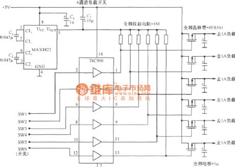
Composed of MAX1822 and 74C906 1~6 channel load switches circuit diagram is shown as below.
MAX1822 is charge pump power supply, its input voltage is in the range of 3.5~16v selection, its output voltage is 11V. You can drive low-impedance N-channel MOSFET. 74C96 is six inverter, SWI~SW6 6 switch signals can be feeded at the same time, alone or in random combinations. This is determinedby requirments for the working condition of load swiches. (View)
View full Circuit Diagram | Comments | Reading(1519)
Separately excited switching power supply circuit diagram used single-junction transistor as pulse generator
Published:2011/3/27 22:07:00 Author:Nicole | Keyword: switching power supply, single-junction transistor, pulse generator
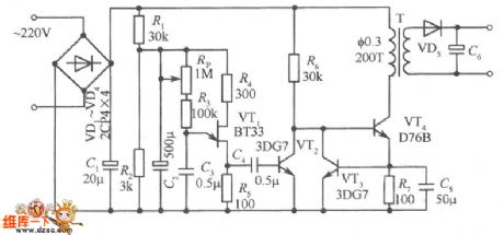
As shown: VD1 ~ VD4 and C1 is the rectifier filter circuit, turning the 220V AC mains voltage into 300V DC. Pulse generator consists of a single junction transistor VT1, resistors R3, R4, R5, potentiometer RP and capacitor C3, with the change of potentiometer's resistance, the pulse frequency is changed. C4 for coupling capacitor of the output pulse. Rl and R2 make 300V DC divider to a single-junction transistor VTl, and provide 20 ~ 30V operating voltage. VT2 is the inverting amplifier tube, inverted and amplified the output positive pulse of the pulse generator, transport a negative pulse to switch VT4, so that it is ended when VT1 output positive pulse.
VT3, R7, C5 form the protection circuit of switch VT4. When connected to power supply, and the pulse generator has not worked, VT4 is on, the pressure drop on R7 increases, make the base bias of VT3 increase, cause the collector current Ic3 increased, the pressure drop Uce3 reduced, base potential of VT4 tube decreased, limiting the collector current of VT4 Ic4, so that it is remained in the security value.
(View)
View full Circuit Diagram | Comments | Reading(2566)
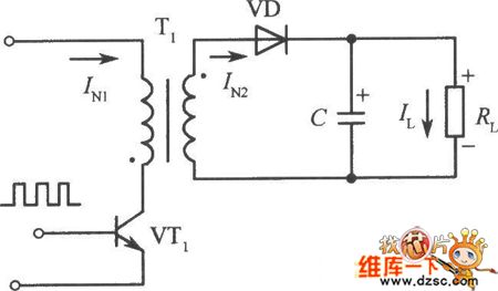
Buck chopped wave switching power supply circuit diagram
Published:2011/3/24 21:42:00 Author:Nicole | Keyword: switching power supply
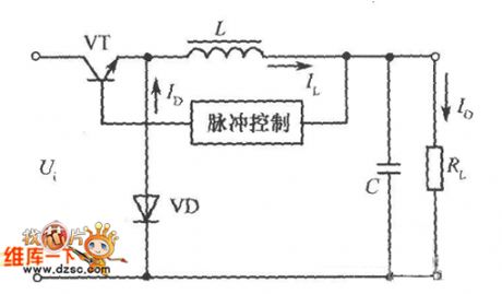
This is a buck chopped wave switching power supply circuit diagram. When the switching element VT is controlled as saturated conduction, the energy is stored in inductor L and capacitor C, and also is fed to the load. When the switching element VT is controlled as cut-off state, the energy stored in inductor and capacitor continue to supply the load, the diode VD constitute a current loop. Because of the switching element VT in series with the load resistor RL, so it is called series switching power supply.
Chopped wave switching power supply is a DC power supply, can obtain unidirectional square wave from switch circuit, and then can get a different steady DC which is different from the input voltage after filtered. The buck is whether the input voltage Ui is positive or negative, the output voltage Uo is always lower than the input voltage Ui, that is | Uo | ≤ | Ui |.
If the adjustment switching element VT has been conducting, the off-time is zero, then Uo = Ui; if VT has been cut-off, on-time is zero, then Uo = 0V. As the ratio of ton and toff is different, the output voltage Uo is between O ~ Ui.
(View)
View full Circuit Diagram | Comments | Reading(942)
5W switching power supply circuit diagram
Published:2011/3/23 2:04:00 Author:Nicole | Keyword: 5W switching power supply
View full Circuit Diagram | Comments | Reading(2397)
60W switching power supply circuit diagram composed of UC3844
Published:2011/3/23 2:05:00 Author:Nicole | Keyword: 60W switching power supply
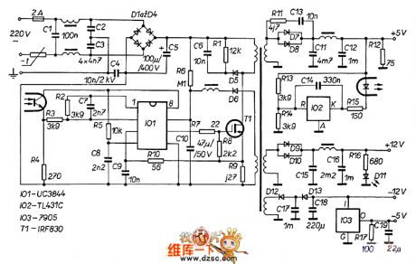
View full Circuit Diagram | Comments | Reading(7667)
ALP-803KDVD Switching power supply circuit diagram
Published:2011/3/29 20:44:00 Author:Rebekka | Keyword: Switching power supply
Here is the schematic diagram of the ALP-803KDVD Switching power supply: (View)
View full Circuit Diagram | Comments | Reading(2281)
Single-ended flyback converter switching power supply circuit diagram
Published:2011/3/24 0:40:00 Author:Nicole | Keyword: converter, switching power supply
Single-ended flyback power converter switching power supply is not composed only by a transistor, the single-ended converter switching power supply also can be made of two transistors. The fundamental difference between Single-ended flyback switching power supply and the push-pull, full bridge, half-double-ended converter switching power supply is that the core of high-frequency transformer only work on one side of its hysteresis loop. The schematic of atypical single-ended flyback converter switching power supply as shown. The so-called single-ended, that means the core of converting circuit only work on one side of its hysteresis loop. The so-called flyback, that means when the transistor turns on, the energy stored in the primary induction coil, when the transistor is off, the energy stored in the primary coil will release to the load through the secondary coil. When the switching tube VT1 was motivated to turn on, the input voltage Ui will be applied to the primary winding N1 of high-frequency transformer T1. Due to the secondary rectifier diodes VD of transformer T1 was reversed, so there is no current flow on the secondary winding N2. When VT1 end, the voltage of winding N2 was polarity reversed, VD was positively skewed, the energy during VTl turns on stored in T1 will released through VD load.
(View)
View full Circuit Diagram | Comments | Reading(3725)
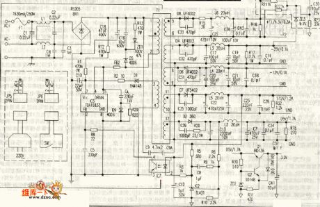
15V/3.5A 52W switching power supply circuit diagram composed of MC33374T/TV
Published:2011/3/23 22:32:00 Author:Nicole | Keyword: 52W switching power supply
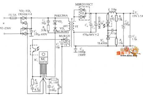
15V/3.5A 52W switching power supply circuit composed of MC33374T/TV as shown. The allowed range of AC input voltage is 92 ~ 276V. Rectifier bridge VD1 ~ VD4 use four 1N5406 3A/600V silicon rectifier tubes. Primary protection circuit is composed of RC absorber circuit (R2, C2) and the clamp circuit (VDz, VD5), it can effectively suppress the peak voltage due to the leakage of high-frequency transformer, to protect the internal power switch of MC33374 from damaged. VDz adopts P6KE200A transient voltage to suppress the diode(TVS), then the reverse breakdown voltage UB = 200V. VD5 uses MURl60 super fast recovery diode (SRD). Note, the serial number of RC R1, C3 in the figure is vacant, according to the need, it can turn the series circuit of R2, C2 into the R1 (20kΩ, 2W) and C3 (0.1μF, 400V) in parallel and then serial ultrafast recovery diode, formed R, C, VD protection circuit.
C5 is the bypass capacitor of Vcc side. S for control switching power supply, the key of on/of. After in series with R7 S, it can improve the reliability of mode conversion. VD6 and C6 form the high-frequency rectifier filter of the feedback coil output. Secondary high-frequency rectifier uses Schottky diode with high current, low voltage the model is MBR20100CT (20A/100V). The tube is common cathode, the two negative electrodes (cathode) are short circuited interiorly, it needs the two positive(anode) connected in parallel externally. C8, C11, L, C12 and C13 form the output filter circuit. In view of the inductance of filter inductance L is small, only 5.0μH, and large-capacity filter capacitors C8, Cl1 have equivalent inductance Lo, it will directly affect the actual inductance from L into L + Lo, so it should take the voice φ0.55mm enamelled wire with 7-turn around the feeder ring N3, and around the middle of the frame, to reduce leakage; also should around two layers of polyester film. The model of ferrite core is E25. In order to prevent saturated magnetization, it should stay out of the air gap of 0.43mm between the two E-shaped cores.
(View)
View full Circuit Diagram | Comments | Reading(4644)
Low power switching power supply circuit diagram
Published:2011/3/22 2:25:00 Author:Nicole | Keyword: switching power supply
View full Circuit Diagram | Comments | Reading(804)
Skyworth 3T30 color TVs switching power supply circuit diagram
Published:2011/3/22 2:24:00 Author:Nicole | Keyword: Skyworth, switching power supply
View full Circuit Diagram | Comments | Reading(2036)
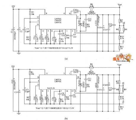
Multiple integrated switching regulator L4970A/L4975A/L4977A(L4972A/L4974A) circuit diagram
Published:2011/3/22 1:18:00 Author:Nicole | Keyword: integrated switching regulator
View full Circuit Diagram | Comments | Reading(3880)
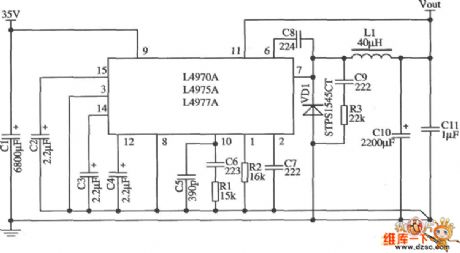
5.1V regulator circuit diagram composed by L4970A、L4975A、L4977A
Published:2011/3/22 1:13:00 Author:Nicole | Keyword: 5.1V regulator
View full Circuit Diagram | Comments | Reading(3522)
| Pages:7/8 12345678 |
Circuit Categories
power supply circuit
Amplifier Circuit
Basic Circuit
LED and Light Circuit
Sensor Circuit
Signal Processing
Electrical Equipment Circuit
Control Circuit
Remote Control Circuit
A/D-D/A Converter Circuit
Audio Circuit
Measuring and Test Circuit
Communication Circuit
Computer-Related Circuit
555 Circuit
Automotive Circuit
Repairing Circuit