
Low Frequency Signal Generating
Index
The frequency divider circuit with a rate of 18 and made by CD4017
Published:2011/8/14 7:10:00 Author:leo | Keyword: Frequency divider, rate
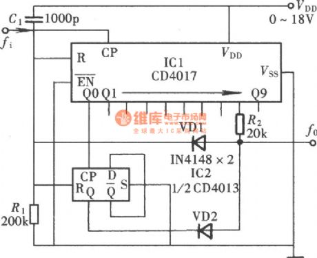
View full Circuit Diagram | Comments | Reading(2330)
VERY_LOW_FREOUENCY_GENERATOR
Published:2009/6/24 2:29:00 Author:May
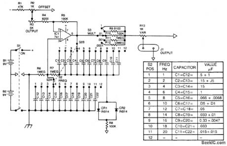
Wien bridge oscillator generates frequen-cies of 1 Hz and 2 to 20 Hz in 2 Hz steps. Maximum output amplitude is 3 volts rms of8.5 volts peak-to-peak. A pot-and-switch at-tenuator allows the output level to be set with a fair degree of precision to any value within a range of 5 decades. (View)
View full Circuit Diagram | Comments | Reading(1246)
Low frequency signal generator(2Hz,4Hz,60Hz,120Hz)
Published:2011/7/29 2:26:00 Author:Ecco | Keyword: Low frequency, signal generator, 2Hz, 4Hz, 60Hz, 120Hz
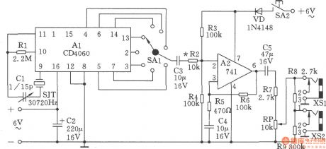
Low frequency signal generator can be used to measure the sensitivity of amplifier, frequency response, frequency compensation, tone control, it is very useful measuring instruments to repair low-frequency amplifier. It is also used as a digital clock source. Depending on the actual use, the signal generator outputs eight fixed frequencies, selecting switch arbitrarily, the voltage output range can be adjusted in two blocks of 0 ~ 0.1V, 0 ~ 1V. The working principle is shown as the chart. IC CD4060 is a fourteen divider with an oscillator. The crystal SJT produces a 30720Hz weak signal frequency, and it forms a crystal oscillator with Cl and the internal of CD4060 inverter. Rl is used to provide feedback loop, it can only produce oscillation on the fundamental frequency of crystal, the oscillation center frequency is 30720Hz. The tuning capacitor Cl makes the frequency tune at the center frequency. SA is placed at pin 3 of CD4060. 30720Hz is divided by CD4060 nine stage(512 times), the pin 13 outputs high accuracy 60Hz output frequency, the capacitor C3 coupled it to the pin 2 of 741 op-amp for signal amplification, then outputed form pin 6 of 741.
(View)
View full Circuit Diagram | Comments | Reading(3235)
Linear voltage-controlled oscillator(8038、μA741) circuit
Published:2011/7/20 23:31:00 Author:leo | Keyword: Linear oscillator, voltage-controlling
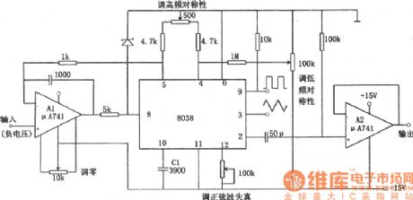
As the picture shows, it is a linear voltage-controlled oscillator circuit. A1 is the constant current power supply circuit used to improve C1, which ensure the linear relationship between output frequency and input controlled voltage. A2 is the sine wave output bumper. If inputting low frequency saw wave to the voltage controlled port, the circuit is changed to linear scan generator and if inputting the voltage of some signal into input port, the circuit outputs frequency-modulated wave.
(View)
View full Circuit Diagram | Comments | Reading(2563)
one point connetion method of amplification circuit
Published:2011/6/27 22:15:00 Author:chopper | Keyword: one point connetion method, circuit
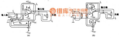
Thus,it needs one point connetion method.The so-called one point connetion means the reference potentials of every part are the same.The picture a,b is the one point connetion method.As the picture (a),the ground of input end and amplifier is connected to the ground of power supply by one line.Therefore,all return current is circulated between the input signal ground and the amplifier.If among the benchmark ground there is a wiring resistor RC,it will generate noise and hum.
(View)
View full Circuit Diagram | Comments | Reading(740)
landlines of low frequency circuit
Published:2011/6/27 21:59:00 Author:chopper | Keyword: landlines, low frequency circuit
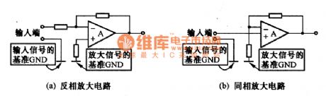
In the low frequency circuit,different grounding methods will effect a lot to the circuit performance when deal with the weak level signal.The picture a,b are the grounding methods of amplifier circuit.The picture (a) is a inverse amplification circuit,and it takes the same phase input terminal of operational amplifier as benchmark by connecting it to ground through resistor to amplify.The picture(b) is a in phase amplification circuit and it takes the inverse input end of operational amplifier as benchmark by connecting it to ground through resistor to amplify.
(View)
View full Circuit Diagram | Comments | Reading(692)
CD4093 sine wave switching to square wave circuit
Published:2011/6/9 21:19:00 Author:John | Keyword: sine wave, square wave
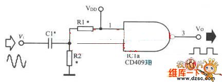
The input sine wave voltage supplies power to IC1 through the half-wave double voltage circuit, which is composed of C1, C2 and D1, D2. IC1A constitutes amplifier in order to amplify the input signal. The signal would be transformed into a square wave signal through the IC1B and IC1C. Then square wave signalis output after the amplification by IC1D, IC1E and IC1F. R2 is used to adjust the output signal amplitude. The circuit as shown can output square wave with good performance within the 20Hz-20KHz. During the application, the valid value for the input sine wave is suggested to be greater than 1.5 volts in order to ensure the quality of the output signal. Minimum input voltage sine wave must be greater than 750mV and the peak value for output signal is about 2 volts at this time.
Figure 1 sine wave switching to square wave circuit (View)
View full Circuit Diagram | Comments | Reading(4135)
OCL drived by NPN tube circuit
Published:2011/6/8 20:07:00 Author:chopper | Keyword: OCL, NPN
View full Circuit Diagram | Comments | Reading(716)
Direct FM Modulation Circuit Diagram composed of Varactor Diode
Published:2011/5/5 9:46:00 Author:Felicity | Keyword: Direct FM Modulation Circuit Diagram, Varactor Diode,
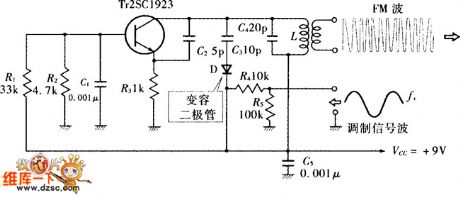
View full Circuit Diagram | Comments | Reading(3925)
Low frequency signal generator with high performance and composed of F007
Published:2011/4/21 6:00:00 Author:Ecco | Keyword: Low frequency, signal generator , high performance
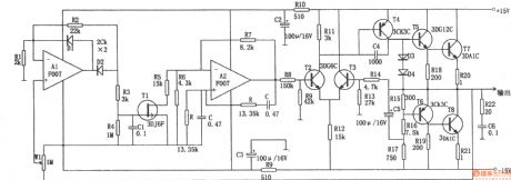
The chart shows the low frequency signal generator circuit with high performance. The circuit is characterized by a steady increase performance, high output power, low waveform distortion. It is an ideal source of low frequency measurement signal. In the figure, the op amp A and its feedback network form a typical Wien oscillator, the oscillation frequency: f0 = 1/2. The output of RCA2 connecting to the OCL complementary push-pull amplifier may improve the circuit's load capacity. Operational amplifier A1 connected as the negative half-wave amplifier, and it forms a steady negative feedback circuit by combining with W1, R4, C1, T1 and other components. Potentiometer W1 adjusts the output rate, and it is used as sampler in the feedback loop. In order to ensure small waveform distortion, generally it should make R1C1 ≥ 20πRC. The circuit output amplitude is 0.5 ~ 5V, output current is 0 ~ 1A, the frequency adjustment range is 10Hz ~ 10kHz, the output resistance is less than or equal to 0.05Ω, harmonic distortion is less than 0.1%.
(View)
View full Circuit Diagram | Comments | Reading(3489)
Circuit Categories
power supply circuit
Amplifier Circuit
Basic Circuit
LED and Light Circuit
Sensor Circuit
Signal Processing
Electrical Equipment Circuit
Control Circuit
Remote Control Circuit
A/D-D/A Converter Circuit
Audio Circuit
Measuring and Test Circuit
Communication Circuit
Computer-Related Circuit
555 Circuit
Automotive Circuit
Repairing Circuit