
Basic Circuit
Index 392
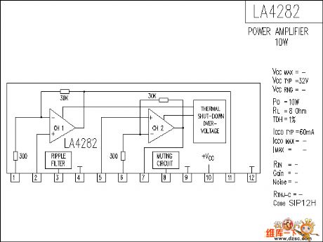
LA4282 audio IC circuit diagram
Published:2011/6/28 2:56:00 Author:Ecco | Keyword: audio IC
View full Circuit Diagram | Comments | Reading(2962)
Infrared remote control switch circuit diagram
Published:2011/6/28 2:53:00 Author:Ecco | Keyword: Infrared , remote control , switch
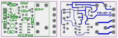
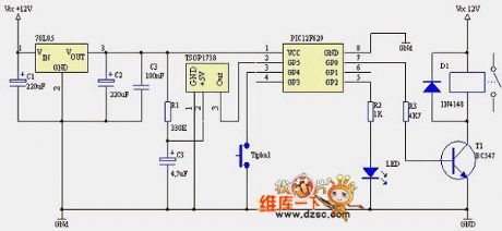
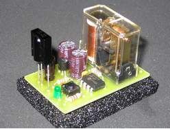
Making such a remote control switch is very simple, even beginners can do it well, because this circuit is too simple, and it only requires a dozen components. The SCM is used as the processing chip, so the circuit is simple. The SCM uses PIC12F629, and the integrated remote control receiver uses TSOP1738, of course, if you do not find this type of receiver, you can use an alternative model, and the relay chooses 12V relay.
(View)
View full Circuit Diagram | Comments | Reading(2517)
CF155 Double-Power High Input-Impedance Single-Supply Amplifier Circuit Diagram
Published:2011/6/26 9:22:00 Author:Vicky | Keyword: Double-Power High Input-Impedance Single-Supply
CF155 series operational amplifier’s output circuit is composed by MOSFET. Its features are: low input current, low power supply current, low power dissipation, low noise, low offset voltage, and exterior zero-setting end. It is available in high-speed integrator, sampling/maintaining circuit of quick-speed D/A converter. The analog types or substitutions are: CFl55MT、CF255LT、CF355CT、CFl55MD、CF255LD、CF355CD、CFl55MJ、CF255LJ、CF355CJ、CF355CP. The above pictures are CF155 typical applied circuit: picture(a) is inverting amplifying and zero-setting circuit, and picture(b) is differential input and zero-setting circuit. (View)
View full Circuit Diagram | Comments | Reading(702)
AN6367NS chrominance signal processing integrated circuit
Published:2011/6/29 1:18:00 Author:Christina | Keyword: chrominance signal, processing integrated circuit

The AN6367NS chrominance signal processing integrated circuit is produced by the Panasonic company that can be used in the Panasonic NV-M series cameras.
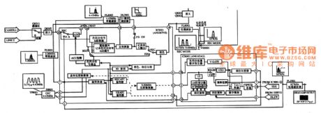
1.Features
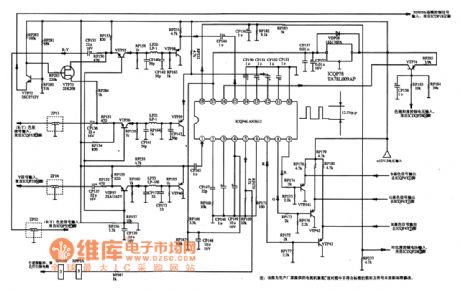
The internal main function of the AN6367NS is to produce the 5.06MHz signal by the vice converter, and supply the record and playback chromaticity signal transformation for the main converter, also it has the automatic frequency phase control function during the recording. The internal circuit block diagram of the AN6367NS is as shown in figure 1.
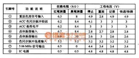
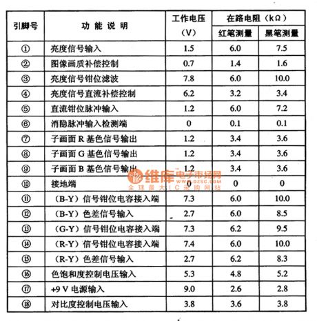
2.Pin functions and data
The AN6367NS is in the 22-pin dual-row plastic structure, the pin functions and data are as shown in table 1.
Table 1 The pin functions and data of the AN6367NS
3.The typical application circuit
The typical application circuit of the AN6367NS is as shown in figure 1.
Figure 1 The typical application circuit of the AN6367NS
(View)
View full Circuit Diagram | Comments | Reading(510)
AN6363AS chrominance signal processing integrated circuit
Published:2011/6/29 1:30:00 Author:Christina | Keyword: chrominance signal, processing integrated circuit
The AN6363AS chrominance signal processing integrated circuit is produced by the Panasonic company that can be used in the Panasonic NVM series cameras.
1.Features
The internal main function of the AN6363AS is to produce the interval phase line-by-line phase shifting 90°627KHz signal by the rotator, and the automatic frequency control of the time base correction circuit. The internal circuit block diagram of the AN6363AS is as shown in figure 1.
Figure 1 The internal circuit block diagram of the AN6363AS
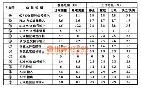
2.Pin functions and data
The AN6363AS is in the 18-pin dual-row plastic structure, the pin functions and data are as shown in table 1.
Table 1 The pin functions and data of the AN6363AS
3.The typical application circuit
The typical application circuit of the AN6363AS is as shown in figure 1. (View)
View full Circuit Diagram | Comments | Reading(492)
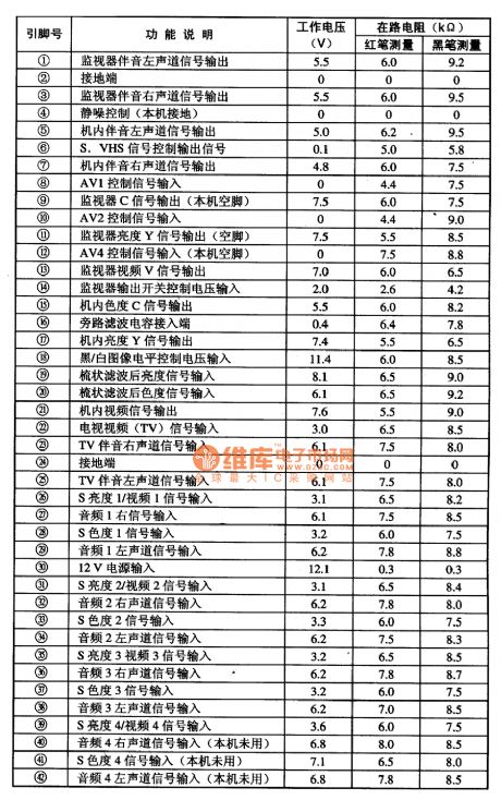
AN5858K TV/AV switching control integrated circuit
Published:2011/6/29 2:11:00 Author:Christina | Keyword: TV/AV, switching control, integrated circuit
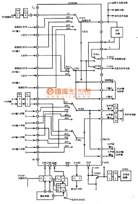
The AN5858K is designed as one kind of multi-channel electronic switch integrated circuit that can be used in the audio and video signal switching applications such as the large screen color TVs.
1.Internal circuit block diagram
The AN5858K has 4 channels of selector switch circuit, the internal circuit block diagram is as shown in figure 1.
Figure 1 The internal circuit block diagram of the AN5858K
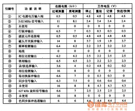
2.Pin functions and data
The AN5858K uses the 42-pin dual-row DIP package, the pin functions and data are as shown in table 1.
Table 1 The pin functions and data of the AN5858K
(View)
View full Circuit Diagram | Comments | Reading(1568)
3DU series silicon phototransistor package type and dimension circuit
Published:2011/6/28 6:45:00 Author:Christina | Keyword: 3DU series, silicon phototransistor, package type, dimension circuit
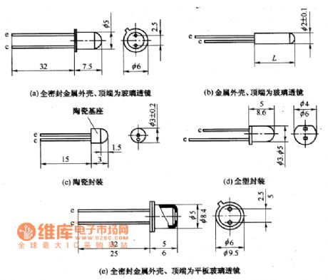
The 3DU series silicon phototransistor can be used in the nearing infrared detector circuit, the optical coupling circuit, the encoder circuit, the characteristic identification circuit, the process control circuit and the laser receiving circuit.etc. The package type and dimension of it are as shown in the figure.
Figure The3DU series silicon phototransistor package type and dimension circuit (View)
View full Circuit Diagram | Comments | Reading(1014)
AN5612 chromatic aberration/fundamental color conversion integrated circuit
Published:2011/6/29 2:28:00 Author:Christina | Keyword: chromatic aberration, fundamental color, conversion, integrated circuit
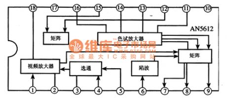
The AN5612 chromatic aberration/fundamental color conversion integrated circuit is produced by the Panasonic company that can be used in the large screen and picture in picture color TVs such as the ChangHong NC-3 series color TVs.
1.Features
The AN5612 has the functions of video signal amplification, chromatic aberration signal amplification and the G-Y signal matrix. The pin-2 of this IC is connected with the control regulating components to improve the video signal at the frequency of 2~3MHz. In addition, the line & field blanking pulse has the function of color signal blanking. The internal circuit block diagram is as shown in figure 1.
2.Pin functions and data
The AN5612 uses the 18-pin dual-row package, the pin functions and data are as shown in table 1.
Figure 1 The internal circuit block diagram
Table 1 The pin functions and data of the AN5612
3.The typical application circuit
The typical application circuit of the AN5612 is as shown in figure 2.
(View)
View full Circuit Diagram | Comments | Reading(1182)
Phototransistor circuit
Published:2011/6/29 2:47:00 Author:Christina | Keyword: Phototransistor
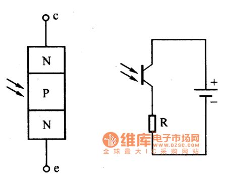
If you connect the phototransistor in this circuit, the collector of the phototransistor is connected with the positive potential, the emitter of it is connected with the negative potential. When there is no light irradiation, the current which flows through the phototransistor is the Iceo between the electrode and the emitter of the phototransistor, it is the dark current of the phototransistor: Iceo=(l+hFE)Icbo.
In this formula:
Lcbo--the saturated current between the collector electrode and base electrode;hFE--the DC amplification coefficient of the common-emitter.
The phototransistor has the higher sensitivity than the photosensitive diode.
(View)
View full Circuit Diagram | Comments | Reading(1766)
Phototransistor chip structure schematic circuit
Published:2011/6/29 3:26:00 Author:Christina | Keyword: Phototransistor, chip structure, schematic circuit
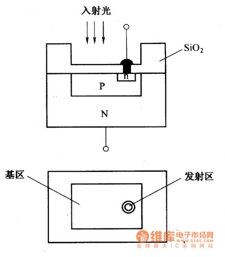
The phototransistor is the same as the conventional semiconductor transistor. It is the semiconductor tube that has the NPN or PNP structure with the semiconductor technology. The structure of it is similar with the semiconductor - diode, the extraction electrode of it is only one or two.
The phototransistor structure is as shown in the figure. In order to adapt to the requirements of the photoelectric conversion, the base region area is large, the launch region area is small. The incident light is mainly absorbed by the base region. The same with the phototransistor, the chips of the tube are installed in the metal shell, the light irradiates on the chips through the lens.
Figure: The Phototransistor chip structure schematic circuit (View)
View full Circuit Diagram | Comments | Reading(1161)
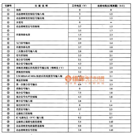
AN5342K picture definition enhancing integrated circuit
Published:2011/6/29 3:46:00 Author:Christina | Keyword: picture, definition, enhancing, integrated circuit
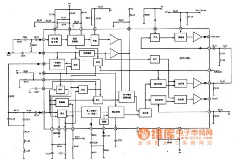
The AN5342K is designed as one kind of picture definition enhancing integrated circuit that is produced by the Panasonic company, and it can be used in the domestic and imported large screen color TVs.
1.Features
The AN5342K is composed of the full wave rectifier cutting circuit, the wave detection controller circuit, the brightness detection circuit, the one-time differentiator circuit, the gain control circuit, the details gain control circuit, the summator, the limiter, the second-time differentiator and other auxiliary circuits. The internal circuit block diagram of the AN5342K is as shown in figure 1.
Figure 1 The internal circuit block diagram of the AN5342K
2.Pin functions and data
The AN5342K uses the 30-pin dual-row DIP plastic package, the pin functions and data are as shown in table 1.
Table 1 The pin functions and data of the AN5342K
(View)
View full Circuit Diagram | Comments | Reading(732)
MB3752 adjustable regulator, main features and pin of DC-DC circuit and power supply monitor
Published:2011/6/21 6:41:00 Author:Lucas | Keyword: adjustable, regulator, main features , pin , DC-DC , power supply monitor
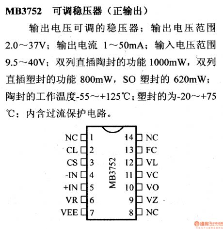
MB3752 adjustable regulator(positive output)
The regulator has the adjustable output voltage; output voltage range is 2.0 ~ 37V; Output Current is 1 ~ 50mA; input voltage range is9.0 ~ 40V; dual in-line ceramic seal function is 1000mW, plastic dual in-line function is 800mW, SO plastic is 620mW; ceramic seal operating temperature is -55 ~ +125 ℃, plastic seal is -20 ~ +75 ℃; it contains over-current protection circuit.
(View)
View full Circuit Diagram | Comments | Reading(591)
The application circuit diagram of capacitive sensor signal regulator
Published:2011/6/27 4:45:00 Author:Ecco | Keyword: application circuit , capacitive sensor, signal regulator
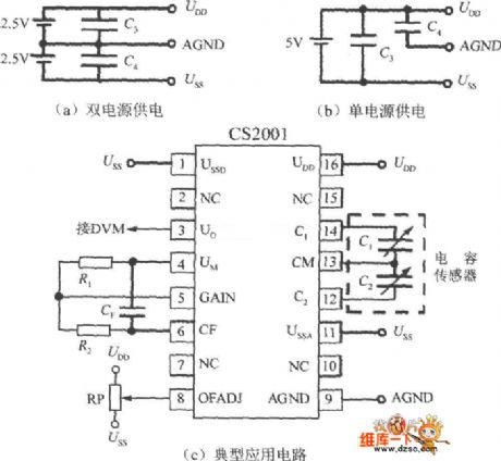
Typical application circuit of CS2001 is shown as the chart. The picture (A) shows the wiring circuit of ± 2.5V dual power supply, and (b) shows the wiring circuit of single +5 V power supply. C3, C4 are decoupling capacitors. In the figure (C), CF is the capacitor for adjusting the bandwidth, and RP is potentiometer to adjust the gain. The output voltage of CS2001 is leaded from Uo, AGND end and connected to the digital voltmeter (DVM).
(View)
View full Circuit Diagram | Comments | Reading(828)
MC34063 step-down expansion flow designing circuit diagram
Published:2011/6/28 2:33:00 Author:Ecco | Keyword: step-down , expansion flow, designing
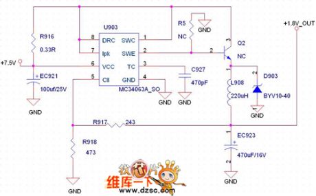
View full Circuit Diagram | Comments | Reading(6229)
Antig 15 W electronic ballast circuit diagram
Published:2011/6/28 2:24:00 Author:Ecco | Keyword: Antig, 15 W , electronic ballast
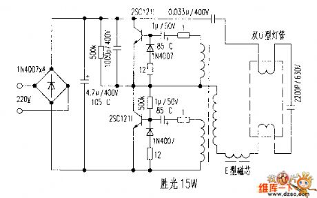
View full Circuit Diagram | Comments | Reading(1163)
40 W electronic ballast electric principle circuit diagram
Published:2011/6/28 2:21:00 Author:Ecco | Keyword: 40 W , electronic , ballast, electric principle
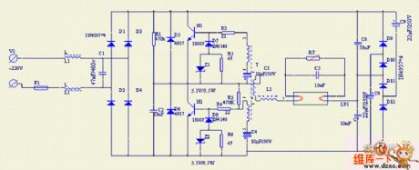
View full Circuit Diagram | Comments | Reading(2026)
A single pipe electronic ballast circuit diagram
Published:2011/6/28 2:54:00 Author:Ecco | Keyword: single pipe , electronic ballast
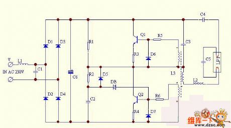
View full Circuit Diagram | Comments | Reading(1482)
LA4192 audio IC circuit diagram
Published:2011/6/28 2:42:00 Author:Ecco | Keyword: audio IC
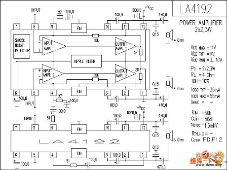
View full Circuit Diagram | Comments | Reading(3801)
LA4190 audio IC circuit diagram
Published:2011/6/28 2:42:00 Author:Ecco | Keyword: audio IC
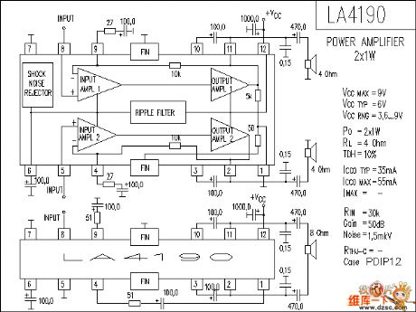
View full Circuit Diagram | Comments | Reading(1678)
AN7222 frequency modulation & amplitude modulation power amplifier integrated circuit
Published:2011/6/28 2:48:00 Author:Christina | Keyword: frequency modulation, amplitude modulation, power amplifier, integrated circuit
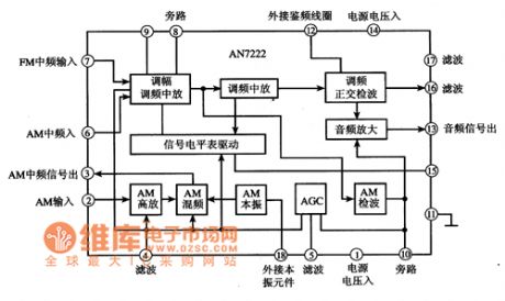
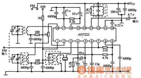
The AN7222 is designed as one kind of frequency modulation & amplitude modulation power amplifier integrated circuit that can be used in all kinds of audio system radio circuits such as the home audio and car audio systems.
1.Features
The AN7222 has the AM detection and FM detection circuits, both of them have the level driver circuit; it has the automatic frequency control function, because of the AM high frequency amplifier, the sensitivity is good, the power consumption is low, and the external components are few. The internal circuit block diagram is as shown in figure.
Figure 1 The internal circuit block diagram of AN7222
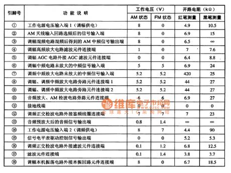
2.Pin functions and data
The AN7222 uses the 18-pin dual-row DIP package, the pin functions and data are as shown in table 1.
Table 1 The pin functions and data of the AN7222
3.The typical application circuit of the AN7222
(View)
View full Circuit Diagram | Comments | Reading(4713)
| Pages:392/471 At 20381382383384385386387388389390391392393394395396397398399400Under 20 |
Circuit Categories
power supply circuit
Amplifier Circuit
Basic Circuit
LED and Light Circuit
Sensor Circuit
Signal Processing
Electrical Equipment Circuit
Control Circuit
Remote Control Circuit
A/D-D/A Converter Circuit
Audio Circuit
Measuring and Test Circuit
Communication Circuit
Computer-Related Circuit
555 Circuit
Automotive Circuit
Repairing Circuit