
Basic Circuit
Index 383
Biopotential / frequency converter composed of LM324
Published:2011/7/5 6:54:00 Author:Lucas | Keyword: Biopotential / frequency converter
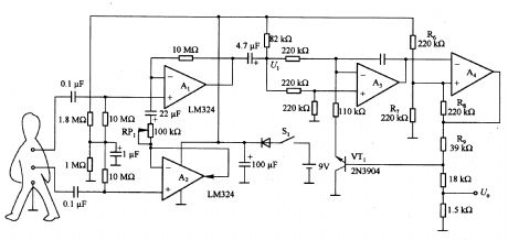
The modulation circuit is composed of the high-gain differential amplifier, and it includes operational amplifiers Al and A2 and related discrete components. Regulating RPl can change the the gain of the electrode amplifier in the range of 100 times to 10,000 times, the biological potential is enlarged to a sufficient level to control the voltage frequency modulation circuit in the modulation circuit. The voltage frequency modulation circuit is composed of the reversible integrator A3 and two-level comparator A4. The integral slash increasing rate of A3 is 227xUl (V / μS), and the increasing positive and negative direction is decided by the VTl the boron dry state, which is controlled by the A4.
(View)
View full Circuit Diagram | Comments | Reading(10583)
A simple micro power transmitter field intensity indicator circuit diagram
Published:2011/6/30 3:32:00 Author:Ecco | Keyword: simple , micro power , transmitter , field intensity indicator

This circuit is a simple field intensity indicator, which is very sensitive for micro-power signal. Because the circuit is only used for the relative field strength, there is no standard, but you can make debugging easily! You can use the probe to measure modulator output end directly, the probe can measure incentive output.
(View)
View full Circuit Diagram | Comments | Reading(1386)
Touching delay lamp switch circuit(8)
Published:2011/6/30 5:12:00 Author:Ecco | Keyword: Touching , delay lamp , switch
The chart shows the touching delay light switch with good performance , the circuit is characterized by: minimal static power consumption; switch has only two terminals outside, which can replace the ordinary switch. Circuit delay time is mainly decided by C1, R2 discharging time constant. In addition, the trigger sensitivity of VT1 and the magnification of VT2 have a significant impact on the delay time.
(View)
View full Circuit Diagram | Comments | Reading(628)
Touching delay lamp switch circuit(7)
Published:2011/6/30 5:21:00 Author:Ecco | Keyword: Touching , delay lamp , switch
The circuit shown in the chart is the delay lamp which uses the principle of self-oscillation to improve trigger sensitivity. The circuit is composed of the self-excited multivibrator, touch switch, power supply circuit and thyristor switch. The circuit delay time is mainly determined by C1, R4 discharging time constant, and at the same time the R3's resistance, VT1 magnification and touching time also have an impact on the delay time.
(View)
View full Circuit Diagram | Comments | Reading(1496)
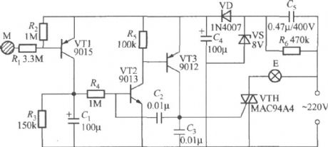
Touching delay lamp switch circuit(6)
Published:2011/6/30 5:17:00 Author:Ecco | Keyword: Touching, delay lamp, switch
In the circuit shown as the chart, the delay time is mainly decided by R5, C discharging time constant, VT1 magnification and the length of touching time. Typically, a manual touching on M, light E can be lit for 1 ~ 2min.
(View)
View full Circuit Diagram | Comments | Reading(569)
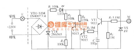
Touching delay lamp switch circuit(5)
Published:2011/7/1 2:34:00 Author:Ecco | Keyword: Touching , delay lamp , switch

The chart shows the touching delay lamp switch circuit with only two outside Lead which can directly replace an ordinary switch to be connected to lighting circuits. The circuit delay time is mainly decided by C1, R3 charging time constant, their value can be adjusted to change the lights lighting duration time.
(View)
View full Circuit Diagram | Comments | Reading(923)
Diode dimmer switch circuit
Published:2011/6/30 2:31:00 Author:Ecco | Keyword: Diode , dimmer, switch circuit
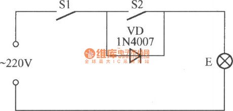
In the circuit shown as the chart, when the S1, S2 are closed, light E has normal light; S1 remains closing, S2 is open, E emits dark light; if S1 is open, the light E is off whether S2 is open or not.
(View)
View full Circuit Diagram | Comments | Reading(1160)
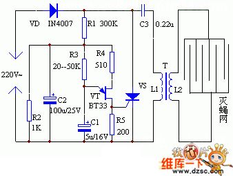
Batch-type cockroach killer circuit
Published:2011/7/5 21:28:00 Author:Christina | Keyword: Batch-type, cockroach, killer circuit
The batch-type cockroach killer circuit is as shown in the figure. It uses the DC voltage to kill the cockroaches. But because the cockroaches are very sensitive to the electric field, they can not climb the high-voltage power net, so this circuit is the batch-type.
(View)
View full Circuit Diagram | Comments | Reading(2110)
MAX882 linear regulator, main features and pin of DC-DC circuit and power supply monitor
Published:2011/6/30 6:06:00 Author:Lucas | Keyword: linear regulator, main features , pin , DC-DC , power supply monitor
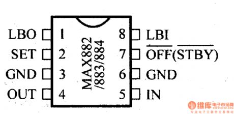
MAX882/ MAX883/MAX884 linear regulator
Output current is 200mA. Input voltage range is 2.7 ~ 11.5V. Output voltage is 3.3V (MAX882 / MAX883) and 5V (MAX884) or adjustable between 1.25 ~ 11V. The voltage will be 200mV when the current is 220mA. Quiescent current is 1 μA, standby mode current is 7μA. It has overload protection function.
(View)
View full Circuit Diagram | Comments | Reading(771)
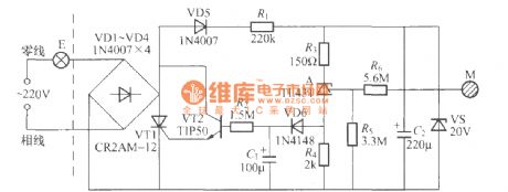
Electronic transformer circuit diagram
Published:2011/6/30 2:39:00 Author:Ecco | Keyword: Electronic , transformer
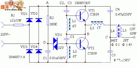
The working principle of electronic transformer is the same with the switching power supply, and it is shown in Figure 1 (click to download the schematic). The VD1-VD4 can recify the electric supply to DC, then DC is changed into tens of kilohertz high-frequency current, which is bucked by ferrite transformer. The R2, C1, VD5 in the figure are start trigger circuit. C2, C3, L1, L2, L3, VT1, VT2 constitute the part of high-frequency oscillation.
(View)
View full Circuit Diagram | Comments | Reading(8845)
The interface circuit diagram of pressure transmitter
Published:2011/7/1 1:38:00 Author:Ecco | Keyword: interface , pressure transmitter
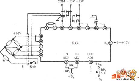
The interface circuit between typical pressure transmitter (such as the Dynisco company's 800 series of pressure transducer) and 1B31 is shown as the chart. 1B31 outputs stable +10 V excitation voltage, and the pressure transmitter full scale output voltage is 30mV. Seting 1B31 gain is 333.3 times could make the 0 to 10,000 lb / inch 2 pressure change into 0 ~ 10V output. For eliminating ground loops, signal returning side and shielded cables must be grounded in the same point. S is the calibration switch, and R is the branch calibration resistor, which can correct full scale output in 80%.
(View)
View full Circuit Diagram | Comments | Reading(1823)
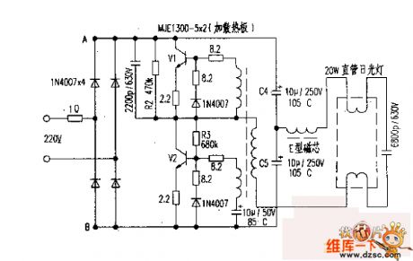
Maintenance circuit diagram of Quartz lamp circuit
Published:2011/7/1 2:57:00 Author:Ecco | Keyword: Maintenance , Quartz lamp
Quartz lamp is widely used in various indoor places of decorative lighting with the advantages of high brightness, condenser, beautiful luxurious, easy installation, low loss, high efficiency. The final stage of the circuit is a buck converter circuit transformer. 220V AC is rectified and inverted to generate about 30kHz ~ 40kHz, 12V AC to light quartz lamp (physical mapping circuit is seen as photo). T is the oscillator output transformer.
(View)
View full Circuit Diagram | Comments | Reading(1209)
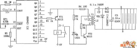
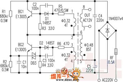
MJE13005 2 electronic ballast circuit diagram
Published:2011/7/1 1:49:00 Author:Ecco | Keyword: electronic ballast
View full Circuit Diagram | Comments | Reading(5971)
MB3756 multiple output regulator, main features and pin of DC-DC circuit and power supply monitor
Published:2011/6/30 20:05:00 Author:Lucas | Keyword: multiple output , regulator, main features , pin, DC-DC , power supply monitor
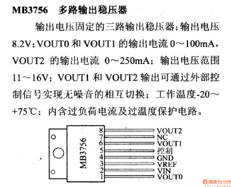
Three ways of output regulator with fixed output voltage; output voltage is 8.2V; VOUTO and VOUT1 output current is 0 ~ 100mA, VOUT2 output current is 0 ~ 250mA; output voltage range is 11 ~ 16V; VOUT1 and VOUT2 output can achieve noise-free switching by external control signal; Operating Temperature is -20 ~ +75 ℃; it includes overload current and over temperature protection circuit.
(View)
View full Circuit Diagram | Comments | Reading(960)
MB3769 switch control circuit, main features and pin of DC-DC circuit and power supply monitor
Published:2011/6/30 5:49:00 Author:Lucas | Keyword: switch control main features , pin , DC-DC , power supply , monitor
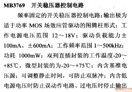
MB3769 switching regulator control circuit It's the switching regulator control circuit with fixed frequency; output is very suitable for power MOS FET-driven totem-pole form; supply voltage range is 12 ~ 18V; the driven load capacity is ± 100mA, ± 600mA; work frequency range is 1 ~ 500KHZ, power is 1000mW; the operating temperature of dual in-line package is -20 ~ +85 ℃, micro-encapsulation is -20 ~ +75 ℃; it includes reference voltage source, which is adjustable dead-time to prevent double pulse; it contains a low voltage power supply circuit to prevent malfunction, stop output during over-voltage.
(View)
View full Circuit Diagram | Comments | Reading(1138)
MB3773 power supply voltage monitoring circuit, main features and pin of DC-DC circuit
Published:2011/6/28 5:56:00 Author:Lucas | Keyword: power supply , voltage monitoring , main features , pin , DC-DC circuit
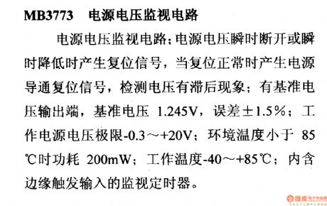
MB3773 power supply voltage monitoring circuit
The instantaneous disconnecting and decreasing of supply voltage will generate the reset signal, when the reset being normal will produce power supply turn-on reset signal, and detection voltage has hysteresis; it has reference voltage output end, and the reference voltage is 1.245V, and error is ± 1.5%; T is the power supply with the limit in -0.3 ~ +20 V; when the ambient temperature is less than 85 ℃, the power consumption is 200mW; Operating Temperature is -40 ~ +85 ℃; it contains edge-triggered input monitoring timer.
(View)
View full Circuit Diagram | Comments | Reading(590)
MC1403 voltage circuit, main features and pin of DC-DC circuit and power supply monitor
Published:2011/6/22 6:22:00 Author:Lucas | Keyword: voltage circuit, main features , pin , DC-DC circuit , power supply monitor
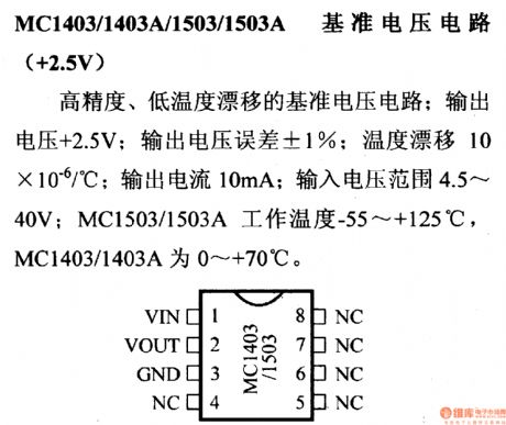
MC1403/1403A/1503/1503A voltage reference voltage circuit(+2.5 V) It's a high-precision, low temperature-drift reference voltage circuit; output voltage is +2.5 V; output voltage error is ± 1%; temperature drift is 10 × 0.000001 / ℃; output current is 10mA ; input voltage range is 4.5 ~ 40V; MC1503/1503A Operating Temperature is -55 ~ +125 ℃, MC1403/1403A is 0 ~ +70 ℃. (View)
View full Circuit Diagram | Comments | Reading(849)
MC1404 voltage circuit, main features and pin of DC-DC circuit and power supply monitor
Published:2011/6/22 6:28:00 Author:Lucas | Keyword: voltage circuit, main features , pin , DC-DC circuit , power supply monitor
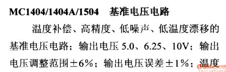
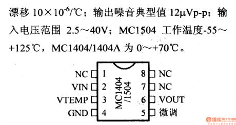
MC1404/1404A/1504 voltage reference voltage circuit
The circuit is a temperature-compensation, high-precision, low-noise, low-temperature drift reference voltage circuit; output voltage is 5.0, 6.25, 10 V; output voltage adjustment range is ± 6%; output voltage error is ± 1%, temperature drift is 10 × 0.000001 / ℃; the typical value of output noise is 12μVp-p; input voltage range is 2.5 ~ 40V; MC1504 operating temperature is -55 ~ +125 ℃, MC1404/1404A is 0 ~ +70 ℃.
(View)
View full Circuit Diagram | Comments | Reading(551)
Voltage/current conversion circuit composed of LM301
Published:2011/7/5 8:39:00 Author:Lucas | Keyword: Voltage/current conversion
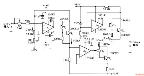
It is the conversion circuit, which can transform ±10V voltage into ±lmA, and the input voltage is changed into current by the A1 and VTl, VT2, and it is used to change the current direction. The input end is added 2mA bias current, when the input voltage is OV, there is 2mA current flowing; the output termination is added 2mA constant current source circuit to offset the input bias current. When the output end is short-circuit, adjusting the potentiometer RP1 make the output current in OA;when the input voltage is + lOV, adjusting potentiometer RP1 make the output current in lmA.
(View)
View full Circuit Diagram | Comments | Reading(3571)
Electronic flykilling device circuit
Published:2011/7/5 20:58:00 Author:Christina | Keyword: Electronic, flykilling device
This electronic flykilling device is very simple and effective .
(View)
View full Circuit Diagram | Comments | Reading(726)
| Pages:383/471 At 20381382383384385386387388389390391392393394395396397398399400Under 20 |
Circuit Categories
power supply circuit
Amplifier Circuit
Basic Circuit
LED and Light Circuit
Sensor Circuit
Signal Processing
Electrical Equipment Circuit
Control Circuit
Remote Control Circuit
A/D-D/A Converter Circuit
Audio Circuit
Measuring and Test Circuit
Communication Circuit
Computer-Related Circuit
555 Circuit
Automotive Circuit
Repairing Circuit