
Control Circuit
Index 4
American siren alarm circuit
Published:2014/1/24 20:22:00 Author:lynne | Keyword: American siren alarm circuit,
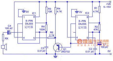
The circuit simulation an American siren sounds. IC2 is connected to a low-frequency multivibrator, the oscillation period is about 6s. C1 slowly changing ramp waveform applied to the PNP emitter follower Q1, and then applied to FM alarm generator IC1 through R6. IC1 natural center frequency of about 800Hz. Operation of the circuit is: alarm output signal from a low-frequency start, and then gradually rises to a high frequency within 3s, then dropped in the 3s to the original low frequency, and so forth continue. American siren alarm circuit shown in Figure:
(View)
View full Circuit Diagram | Comments | Reading(1564)
Dongfeng Peugeot Citroen Picasso 2.0L car door switch information circuit
Published:2014/1/23 20:29:00 Author:lynne | Keyword: Dongfeng Peugeot Citroen Picasso 2.0L car door switch information circuit,
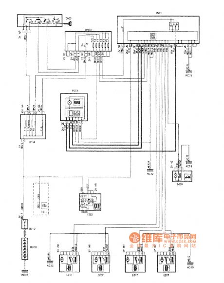
Dongfeng Peugeot Citroen Picasso 2.0L car door switch information circuit shown in Figure:
(View)
View full Circuit Diagram | Comments | Reading(1510)
Soft switching circuit schematic circuit diagram
Published:2014/1/21 21:10:00 Author:lynne | Keyword: Soft switching circuit schematic circuit diagram,
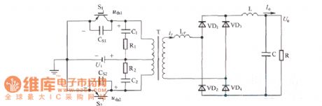
Soft switching circuit schematic circuit diagram shown in Fig.:
(View)
View full Circuit Diagram | Comments | Reading(1184)
Lu lian intelligent remote alarm system electric schematic diagram
Published:2014/1/19 21:52:00 Author:lynne | Keyword: Lu lian intelligent remote alarm system electric schematic diagram,
Lu lian intelligent remote alarm system electric schematic diagram as shown:
(View)
View full Circuit Diagram | Comments | Reading(1731)
Multi-channel burglar alarm circuit diagram
Published:2014/1/19 21:46:00 Author:lynne | Keyword: Multi-channel burglar alarm circuit diagram,
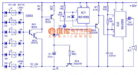
This alarm can be 6-way, from 0 to 30 km on the touch line in both sound and lighting for monitoring. Works in the following figure:Using 6 inverter C033 and light-emitting diodes (leds) as a touch alarm display. When the body contact (directly and/or wear gloves and indirect touch) when any one end in A ~ F, the end brings low potential, the inverter makes light-emitting tube LED display. At this moment, BG1 ~ BG4 conduction, C1 charging, acoustics part (IC1, IC2, etc.) begin to work. IC1, produce about 1 hz sawtooth wave by BG5 buffer to add to the IC2 modulation, IC1 oscillation frequency from low to high, the speaker sends out the similar public security police car alarm.
Use installation should pay attention to the Q end reliable to use A wire from the earth, A ~ F side respectively with bare copper wire to the surveillance, fixed place need porcelain insulation, at the same time pay attention to the rain, water, etc. Between cause and to form A low impedance. The alarm sensitivity is extremely high, standing on a chair touch wires can also call the police, the human body to leave after the all-clear to delay a few seconds. Power supply adopts 8 batteries. Adjust the R6 can change the tone. (View)
View full Circuit Diagram | Comments | Reading(2219)
Vibrating burglar alarm circuit
Published:2014/1/16 21:14:00 Author:lynne | Keyword: Vibrating burglar alarm circuit,
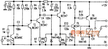
The alarms on the doors and windows using a hidden cheap piezo buzzer X1 as a sensor. This piezoelectric buzzer with bidirectional effect: when a voltage at both ends thereof, the piezoelectric ceramic material which will vibrate and produce a sound mechanical deformation; mechanical hand, when it is subjected to vibrations generated thief sound housebreaking When, at its ends will produce a corresponding output voltage.
>After the use of a property here, making it play a role in vibration sensor. As shown, the voltage generated by the piezoelectric sensor X1 transistor T1 of the first stage amplifier composed of the discharge is about 100 times. Effect transistor T2 from the detector, its collector voltage is only 50mv. Since R3 directly to the base of T2 being connected to the power line, T2 is always in the ON state can not afford to amplification. If you need to increase the magnification, you can change the upper end of R3 T2 collector received. The transistor T3 provides a voltage gain of about 3 times, and the drive pulse detector D1. When the input pulse level is high enough, T4 rapid charging to C6. After the pulse, C6 slow discharge through a high impedance circuit R9 and R10 and T5 base-emitter composed this discharge time determines the turn-on time of the relay. Therefore C6 capacity required by the test needs to decide its value can select between 1uF-10uF. Piezoelectric sensors X1 should use shielded cable to the input of the circuit Swiss, but the cable should be as short as possible. If radio frequency interference, as shown in dotted lines can be shown between the T1 connected to the base and to add a bypass RFI lnF ceramic capacitors. In use, a known vibration source (such as under normal environmental sounds produced) should be kept away from the sensor in order to avoid false triggering. When the relay is not working, the circuit consumes only a few milliamps. Vibrating burglar alarm circuit shown in Figure:
(View)
View full Circuit Diagram | Comments | Reading(1192)
Train lights automatically switch circuit
Published:2014/1/12 21:37:00 Author:lynne | Keyword: Train lights automatically switch circuit,
Train lights automatically switch circuit shown in Figure:
(View)
View full Circuit Diagram | Comments | Reading(985)
Household automatic water supply device circuit principle diagram
Published:2013/12/30 20:56:00 Author: | Keyword: Household automatic water supply device circuit principle diagram,
Household automatic water supply device circuit principle diagram
(View)
View full Circuit Diagram | Comments | Reading(1280)
The length of a probe based on circuit diagram of water vessel
Published:2013/12/30 20:44:00 Author: | Keyword: The length of a probe based on circuit diagram of water vessel,
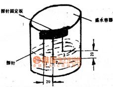
The length of a probe based on circuit diagram of water vessel
(View)
View full Circuit Diagram | Comments | Reading(891)
Household water supply printed circuit diagram
Published:2013/12/30 20:41:00 Author: | Keyword: Household water supply printed circuit diagram,
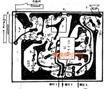
Household water supply printed circuit diagram
(View)
View full Circuit Diagram | Comments | Reading(943)
LDR PC Desk Lamp
Published:2013/12/3 20:40:00 Author:lynne | Keyword: LDR PC Desk Lamp


Most of the PC desk lamps available in the market light up whenever there is an input power. These don’t take into account whether there is a real need for the light or not. Here is an intelligent PC desk lamp circuit that overcome the problem.It senses the light level in the room to determine the actual need for light and lights up only if required. It is designed to work with the PC and remains on only when the PC in the table is in working state. It uses MOC3021.
Front end of the circuit is powered by the 5volt dc supply available from the usb port of the PC. When circuit is powered, the light sensor LDR (R2) resistance is low if there is sufficient light and thus most of the base current of transistor T1 finds an alternative easy path via LDR and T1 remains cutoff. While during dakness, the LDR behaves almost as an open circuit, and the current through sensitivity control preset pot (P1) and assosiated resistors (R1,R3) flows into the transistor’s base. As a consequence, T1 conducts to energise the opto-triac PC1. Next, the lamp driver triac T2 is fired through the opto-triac PC1 and switch on the power supply to the incandescent lamp.
The circuit can be constructed on a medium size PCB. After construction, enclose the finished circuit in a well insulated plastic cabinet. Then drill holes for mounting the ‘B’ type USB input socket, power switching termianls and the LDR etc. This circuit is meant for use in conjuction with Personal Computers to switch on an associated light sensitive table lamp/similar load. An optional electro magnetic relay can also be wired at the output of the circuit to switch heavy electrical load(s). For interconnection between PC and the control circuit, use a standard USB cable with an ‘A’ type connector on one end and a ‘B’ type connector at the other end.
LDR USB Desktop Lamp Circuit Schematic
(View)
View full Circuit Diagram | Comments | Reading(1287)
Light Alarm Circuit with LDR
Published:2013/12/2 21:09:00 Author:lynne | Keyword: Light Alarm Circuit

This musical light alarm circuit is very simple, uses only 7 components, a LDR and a 3.6 V battery or 3 x 1.2 volts rechargeable batteries. The well-known UM66 is used as the sound generator and will give a pleasent wake up alarm.
As you probably know the LDR is a light dependent resistor. Normally the resistance of an LDR is very high, sometimes as high as 1MΩ, but when they are illuminated with light resistance drops dramatically. In the circuit adjust the 220KΩ preset to the desired sensitivity, meaning adjusting the threshold point where the alarm start singing.
When there is light on the light dependent resistor the T1 transistor will start conducting and powers the UM66 musical integrated circuit. The produced musical note will be amplified by transistor T2 and fed into the 8Ω speaker.
On the UM66 IC are different numbers, each number giving a different musical note (in this example we use UM66T). You may use 2 x 1.5V batteries but 3 x 1.2V NiCad or NiMH are better because you can recharge them.
Light alarm electronic circuit schematic
(View)
View full Circuit Diagram | Comments | Reading(1314)
Low Current Relay Circuit
Published:2013/11/28 21:02:00 Author:lynne | Keyword: Low Current Relay Circuit
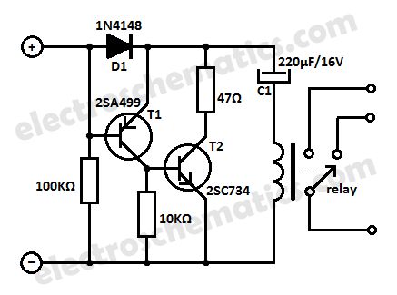
This low current relay circuit is designed to be used in battery operated electronic devices. Its operating current is in micro amperes (µA). This is done by using a bistable relay and adding some components to force the relay to behave like a monostable relay.
A bistable relay stays at its last state when the power is turned off but consume at least 50mA trigger current. A monostable relay switches back to its original state when the power is turned off.
How does the low current relay works?
When the power is turned ON, the C1 charges via D1 and the relay coil and this current activates the relay. D1 ensures that the base of T1 is always more positive than its emitter and because of this T1 and T2 are always blocked.
Once the power is turned OFF, the emitter of T1 is coupled to the charge voltage at the positive pole of C1. Its base and the relay coil on the other hand are coupled to the negative pole of C1 and now T1 and T2 conduct, C1 can discharge through T2 and relay. The current flows to the relay coil but in reverse order so is activated to its other state.
It has the advantage of consuming little current, around 150 µA. For a reliable operation, select the relay’s operating voltage as 2/3 to 3/4 of the main power supply. For example is using a 12V power supply select a 9V relay.
Transistors replacements:T1 = 2SA499 = BC557, BC558T2 = 2SC734 = BC547, BC548
Low current relay switch circuit schematic
(View)
View full Circuit Diagram | Comments | Reading(1584)
Universal Triac Control with Optocouplers
Published:2013/11/28 20:12:00 Author:lynne | Keyword: Universal Triac Control
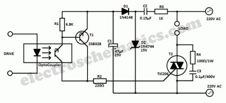
This universal triac controller circuit with optocoupler solves the problem that triacs have when functioning at low temperatures (triac needs higher gate current) by adding a transistor at the output of the optocoupler circuit.The transistor amplifiers the trigger pulse coming from the optocoupler and the gate current is high enough to trigger the triac in all temperature cases.
How does the circuits works?
The base of the transistor is driven by the OC. C2 works as capacitive bias resistance to avoid power losses and it also helps avoid DC loading of the supply line. The switch current is limited by R3. D1 works as one-way rectifier while C1 works as ripple filter.D2 stabilize the rectified voltage to 15 V.
T1 conducts when the OC sends a pulse to its base. C discharges through the collector-emitter line. The trigger current is limited by R2 to around 40 mA.The discharge current time of C1 is less than 1 ms.
The RC circuit R4 and C3 protects the triac from voltage spikes.This is very important in all inductive loads.
Triac Optocoupler Controller Schematic
(View)
View full Circuit Diagram | Comments | Reading(2371)
Universal Triac Control with Optocoupler
Published:2013/11/27 21:07:00 Author:lynne | Keyword: Universal Triac Control with Optocoupler

This universal triac controller circuit with optocoupler solves the problem that triacs have when functioning at low temperatures (triac needs higher gate current) by adding a transistor at the output of the optocoupler circuit.The transistor amplifiers the trigger pulse coming from the optocoupler and the gate current is high enough to trigger the triac in all temperature cases.
google_ad_client= ca-pub-9265205501290597 ;google_ad_slot= 6648404198 ;google_ad_width=336;google_ad_height=280;
How does the circuits works?
The base of the transistor is driven by the OC. C2 works as capacitive bias resistance to avoid power losses and it also helps avoid DC loading of the supply line. The switch current is limited by R3. D1 works as one-way rectifier while C1 works as ripple filter.D2 stabilize the rectified voltage to 15 V.
T1 conducts when the OC sends a pulse to its base. C discharges through the collector-emitter line. The trigger current is limited by R2 to around 40 mA.The discharge current time of C1 is less than 1 ms.
The RC circuit R4 and C3 protects the triac from voltage spikes.This is very important in all inductive loads.
Triac Optocoupler Controller Schematic