
power supply circuit
Index 238
Siganl station power supply distribution system diagram
Published:2011/4/14 2:26:00 Author:muriel | Keyword: Siganl station , power supply, distribution , system diagram
Communication power is the power which isdirectlysupplying to the communication equipment. Communication power isthe key part and subject of the signal station , signal station power supply also includes theguarantee building load of the short time interrupt, such as CRAC etc. General signal station power supply component isas shown. (View)
View full Circuit Diagram | Comments | Reading(721)
100v/1A Regulated voltage circuit
Published:2011/4/14 21:53:00 Author:muriel | Keyword: 100V/1A, Regulated voltage circuit
The circuit only adjusted the part of the output voltagewhich is about the voltage change of total voltage, the total voltage consists of U11 and U1 two parts, the limit voltage value of the transistor are higher than the Uceomax. The circuit has the short overload protection function, two parts of voltage source must have the capability to withstand the maximum load current.
Main technical data:
output voltage:U2=100V
output current:I2=1A
Input voltage: U11=64V to 96V, U1=40V to 60V
Output voltage variation:
When environment temperatureθU=0°C to 60°C, ΔU2=200mV
When output current I2=0A to 1A(U1=constant), ΔU2=45mV
When input current are the above values(I2=0), ΔU2=60mV (View)
View full Circuit Diagram | Comments | Reading(1119)
Regulated votlage micro-switching power supply (3W-10W circuit diagram)
Published:2011/4/22 6:46:00 Author:May | Keyword: Regulated votlage, micro-switching power supply, 3W-10W
View full Circuit Diagram | Comments | Reading(6676)
Photosensitive diode circuit used by optical rotary encoder
Published:2011/5/2 6:05:00 Author:Nicole | Keyword: photosensitive diode, optical rotary encoder
The light which is emitted by tungsten bulb reaches photosensitive tube by lens, cylindrical lens and chromium plating optical coded disc slit. The coded disc is scribed as cyclical binary code, if it is n bits binary code, then it needs n photosensitive tubes arrangement in a straight line behind the light slit. 16 bits requires light slit with 20μm width, 15 bits requires light slit with 40μm width, it has good reliability. When it has light, the ammeter showns 0.1μA; when it has no light, it showns 6~10μA. 3DG6D*2 is composite pipe, it has larger amplification factor, it also is the emitter output. Schmitt trigger is composed of two 3DK2, its function is plastic. When it has light, the output is lower than 0.5V, when it has light, the output can reach +6V. (View)
View full Circuit Diagram | Comments | Reading(1525)
Photosensitive oscillation circuit
Published:2011/4/29 23:16:00 Author:Nicole | Keyword: photosensitive oscillation
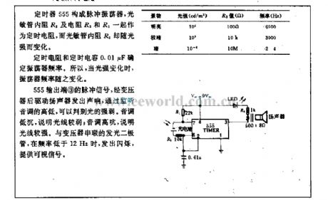
The pulse oscillator is composed of timer 555, the timing resistor consists of photosensitive tube internal resistance R2, resistance R3 and R1, the photosensitive tube internal resistance R2 changes in relation to light intensity.
The oscillator frequency is decided by timing resistor and timing capacitor 0.01μF. So when the light intensity changes, the oscillator frequency changes too.
After transformer drives loudspeaker, the pulse singal of 555 output terminal ③ sends out noise, it can identify the light intensity according to the pitch of monitor tone. If it is low in pitch, then the light is weak; if it is high in pitch, then the light is strong. LED is in series with transformer, when the frequency is lower than 12Hz, it will flash and provide a visible singal. (View)
View full Circuit Diagram | Comments | Reading(605)
Optical coupling SCR circuit
Published:2011/4/29 22:26:00 Author:Nicole | Keyword: Photo coupler, SCR
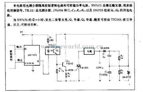
This circuit uses optical coupler to isolate control logic circuit and SCR power circuit. SN7475 is slow trigger, it is used to receive control singal. TIL111 is optical coupler. Q1, Q2 power supply circuit is composed of IN4004, C1, C2, R4, R5 and 1N4733.
When SN7475'S Q=0, LED lights up, Q1 and Q2 turn on, triggering SCR TIC263 to turn on. On the contrary, SCR cuts off. (View)
View full Circuit Diagram | Comments | Reading(2160)
Optical control bolton flash safety light circuit
Published:2011/4/29 22:57:00 Author:Nicole | Keyword: optical control, safety light
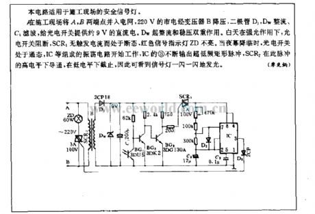
This circuit is suitable for construction site safety light.
In construction site, A, B terminals are connected to power network, 220V mains supply is reduced by transformer B, it is rectified by Dw and filtered by C1, it provides photoelectric switch with 9V DC power. Dw takes the action of rectification and voltage regulation. Under bright light during the day, photoelectric switch cuts off, SCR1 has no trigger current and it is in off state, the red singal indicator light ZD does not turn on. When night comes, photoelectric switch turns on, the oscillation circuit which is composed of IC starts to work, IC's ③ constantly outputs ultra-low frequency rectangular pulse, SCR2 is conduction under this pulse's high level, and it is closed under the low level, so we can see the singal light winking. (View)
View full Circuit Diagram | Comments | Reading(619)
High-power full-bridge converter circuit diagram
Published:2011/4/22 18:42:00 Author:Nicole | Keyword: full-bridge converter
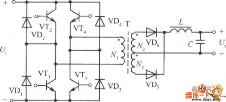
The two electrolytic capacitors of half-bridge converter circuit are changed to the other two high voltage power transistors, and coupled with appropriate drive circuit then can be composed of full-bridge converter circuit, the figure is as shown. VT1, VT2, VT3, VT4 form 4 bridge arms. High frequency transformer T is connected between them. Relative VT1, VT4 and VT2, VT3 alternately inspired by the drive circuit turning on, the DC input voltage into a high-frequency square-wave transform AC voltage. The course of working is the same as push-pull power converter circuit. Thus, when the high frequency transformeris working, the voltage of primary coil is considered to the supply voltage, it is twice the half-bridge circuit output voltage, the pressure of each transistor remains at the supply voltage, twice the output power increases. If the current reach half-bridge circuit, that means the current increases twice, then the output power can increase 4 times. The main disadvantages of full-bridge circuit is thatit needs 4groups transistor base drive circuits which are insulative with each other, complex and increase the cost of the control drive circuit.
(View)
View full Circuit Diagram | Comments | Reading(1127)
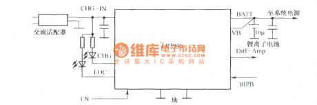
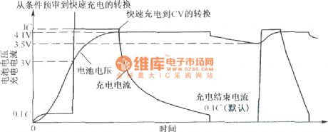
Process of TWL2213 lithium ion battery charging
Published:2011/5/2 7:15:00 Author:Nicole | Keyword: lithium ion battery
Arousal of Li-ion batteries:
Pre-charge circuit:
Fast charge and termination:
Temperature monitoring:
TWL2213 is monitoring the temperature of lithium ion battery all the time during the charging period, and it uses NTC thermal resistor to produce ADC input reference voltage. TWL2213 will compare ADC reference voltage with programmable threshold voltage, then it will decide to stop the process of charging or over heat cutting. (View)
View full Circuit Diagram | Comments | Reading(715)
CCCV Lithium Battery Charge Control Schematic Circuit
Published:2011/4/25 23:59:00 Author:Joyce | Keyword: CCCV, Lithium Battery, Charge Control, Schematic
This is a CCCV lithium battery charging control panel.Q1, R1, W1, TL431 in the figure compose a precise and adjustable constant-voltage circuit. Q2, W2, R2 constitute an adjustable constant-current circuit. Q3, R3,R4 ,R5, LED is a battery charging circuit. As the voltage of the charging lithium battery rises gradually, the charging current will decrease . When the battery is filled, pressure drop on the R4 will gradually decrease till Q3 is cut off, and eventually LED would extinguish. In order to ensure adequate charge of the battery , please continue to charge for 1 ~ 2 hours after the light extinguishes , and install cooling fin of proper size in Q2, Q3 when in use. (View)
View full Circuit Diagram | Comments | Reading(3344)
Independent charger composed of LP3945
Published:2011/4/29 5:09:00 Author:Nicole | Keyword: charger
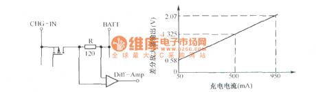
LP3945 is an independent single lithium ion battery charger, it consists of a integrated pass transistor and current detection resistor. Besides charging function, it is also used for low pressure drop pattern. This function is especially useful during the manufacture, bacause it is not needed to connect lithium ion battery when there is product testing and performance verification. The independent charger circuit composed of LP3945 is as below:
The charging period of LP3946 is shown as below:
The charging current induction circuit is shown as below:
(View)
View full Circuit Diagram | Comments | Reading(640)
Linear Voltage Regulator Composed Microprocessor Power Supply Circuit
Published:2011/5/2 1:42:00 Author:Joyce | Keyword: Linear Voltage Regulator Composed, Microprocessor, Power Supply
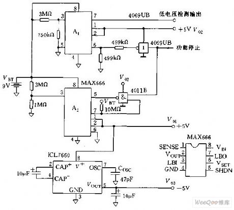
Linear voltage regulators composed microprocessor power circuit is shown in the graph below.It simly consititues of 2 MAX666. Power supply for the CPU and A/D converter is A2,and that for RAM and real-time clock is A1. The output voltage Vo of MAX666 is controlled by VSET , if VSET is connected with GND, the output voltage is 5V,which is fixed. If one uses resistance to part the pressure Vo, the partial voltage will be added to VSET, thus it could be output through programming. (View)
View full Circuit Diagram | Comments | Reading(1142)
LM317-Composed Constant Current and Voltage-stabilized Power Supply Circuit
Published:2011/5/2 2:03:00 Author:Joyce | Keyword: LM317-Composed, Constant Current, Voltage-stabilized, Power Supply
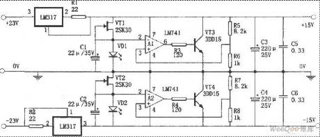
As shown in figure is a constant current and voltage-stabilized power supply connected inparallel,featuring high speed, low noise and low impedance. Using LM317 as its constant current source,it can load constant current up to 560mA . Mosfet 2SR3D and luminotron provide low noise reference voltage. As an error amp,LM741 (amp) would compare and amplify the reference voltage and sampling voltage. In order to stabilize the output voltage,the two 3DD15 are used to adjust the output voltage.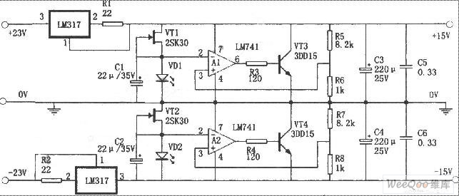 (View)
View full Circuit Diagram | Comments | Reading(4334)
Current source inverter circuit diagram
Published:2011/4/29 5:09:00 Author:Rebekka | Keyword: Current source inverter

Features: L exists. The role of L: filtering and absorption of reactive power for capacitive load. (View)
View full Circuit Diagram | Comments | Reading(3251)
TOPSwitch--Ⅱ
Published:2011/4/21 21:08:00 Author:May
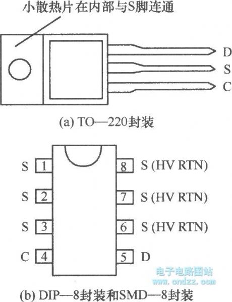
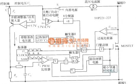
Pin arrangement of TOPSwitch --Ⅱ is shown in the diagram. It has three kinds of package. Among them, TO-220 package has heating panel and belongs to typical three-terminal device. Its shape is the same as 7800 series three-terminal linear regulators. DIP - 8 and SMD-8 package both has 8-pin package, but can be reduced to three; difference between the two is DIP-8 can be equipped with 8 pin IC socket, SMD-8 is surface patch and do not need to punch welding. Three pins of TOPSwitch - Ⅱ are control terminal C (Con-trol), source S (Source), drain D (Drain). TOPSwitch - Ⅱ internal block diagram is shown in below, it mainly includes 10 parts: (1) control voltage source; (2) band gap voltage reference; (3) oscillator; (4) shunt regulator / error amplifier; (5) pulse-width modulator; (6) gate driver stage and output stage; (7) over-current protection circuit; (8) Overheat protection and power-on reset circuit; (9) shutdown / auto-restart circuit; (10 ) high-voltage current source. In the diagram, Zc is control side of the dynamic impedance; RE is error voltage detection resistor; RA and CA make up low-pass filter with 7kHz cut off frequecny. The basic principle of TOPSwitch - Ⅱ is to use the feedback current Ic to adjust the duty cycle D, so as to achieve the purpose of regulation.
(View)
View full Circuit Diagram | Comments | Reading(679)
Nickel-cadmium battery charge protection circuit diagram
Published:2011/4/29 4:20:00 Author:Rebekka | Keyword: Nickel-cadmium battery, charge protection
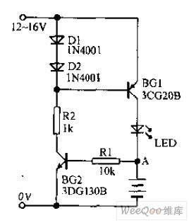
Nickel-cadmium rechargeable battery protection circuit is shown as below. The charging part is composed of D1, D2, R2 and BG1. The charge protection circuit is composed of BG2 and R1. When the nickel-cadmium batteries are charging, light emitting diode LED will be lighten. It indicates charging is normal. If the battery polarity is reversed, base BG2 will be negative potential, BG2 stops, BG1 the base potential will be raised, BG1 stops. It will not charge for nickel-cadmium battery, LED will not lit. It indicates the battery polarity is reversal. (View)
View full Circuit Diagram | Comments | Reading(2839)
Lithium ion battery charging circuit diagram
Published:2011/4/29 4:03:00 Author:Rebekka | Keyword: Lithium ion battery charging
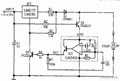
Lithium-ion battery charging circuit is shown as above. When it starts to charge. The battery voltage is below 8.4V, IC1's output has no output. Q2 off, LM317 work in the constant current output. When the battery voltage is increased to 8.4V, Q2 turns on, Q2 controls ADJ-side, so that the output voltage of IC2 significant declines and make the charge current maintain a very small value and the pool in a floating state. (View)
View full Circuit Diagram | Comments | Reading(7248)
Battery fast charge circuit composed of BQ2002 battery fast charge control integrated circuit
Published:2011/4/27 9:16:00 Author:Nicole | Keyword: battery fast charge
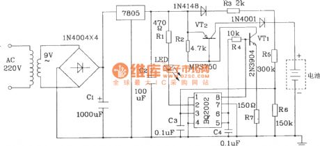
Transformer, diode and steady voltage IC7805 provide this circuit with +5V power voltage, the power voltage is divided by R5, R6 then transported to the BAT terminal of chip, it provides sample voltage. The resistance inputed from reststance partial pressure network to BAT terminal should not be lower than 200kΩ. When TM terminal is grounding, the fast charge rate is 1C, the fast charge supplementary time is 80min. (View)
View full Circuit Diagram | Comments | Reading(3377)
± 15V and ± 26V output power supply circuit diagram
Published:2011/4/29 1:57:00 Author:Rebekka | Keyword: output power supply
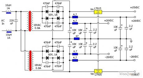
± 15V and ± 26V output power supply circuit diagram is shown as above. (View)
View full Circuit Diagram | Comments | Reading(600)
20A, 13.8V power supply shematic diagram
Published:2011/4/29 3:37:00 Author:Ecco | Keyword: 20A, 13.8V, power supply, shematic diagram

20A, 13.8V power supply shematic diagram is shown as the chart.
(View)
View full Circuit Diagram | Comments | Reading(4800)
| Pages:238/291 At 20221222223224225226227228229230231232233234235236237238239240Under 20 |
Circuit Categories
power supply circuit
Amplifier Circuit
Basic Circuit
LED and Light Circuit
Sensor Circuit
Signal Processing
Electrical Equipment Circuit
Control Circuit
Remote Control Circuit
A/D-D/A Converter Circuit
Audio Circuit
Measuring and Test Circuit
Communication Circuit
Computer-Related Circuit
555 Circuit
Automotive Circuit
Repairing Circuit