
Signal Processing
Index 41
Simple sinusoidal oscillator
Published:2012/8/13 20:56:00 Author:Ecco | Keyword: sinusoidal oscillator
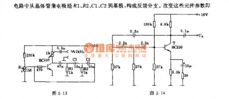
The oscillation signal is adjusted by the potentiometer Rp1. The output resistor is low ( 1kΩ ), so it is applied to a variety of control circuits for the signal source. In the circuit, the transistor collector through R1 , R2, , C1, , C2 to the base and constitutes the feedback branch. Changing the parameters of these components can change the frequency range.
(View)
View full Circuit Diagram | Comments | Reading(1114)
Simple single field-effect transistor oscillator circuit
Published:2012/8/12 22:19:00 Author:Ecco | Keyword: Simple , single , field-effect transistor , oscillator
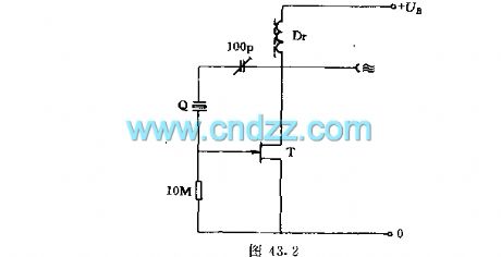
This circuit uses a field-effect transistor to constitute a quartz crystal oscillator circuit with excellent performance, the tuning capacitor is used to adjust the scope, and choke can be selected according to the frequency range to make WL be greater than 20kΩ.
(View)
View full Circuit Diagram | Comments | Reading(1672)
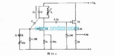
100MHz power oscillator circuit using dual- gate FET
Published:2012/8/12 22:35:00 Author:Ecco | Keyword: 100MHz , power oscillator , dual- gate , FET
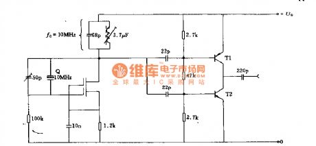
The oscillator uses tuning resonant circuit as the working resistor of the FET. Oscillating power signal is output by the fast switching transistors T1 and T2.
(View)
View full Circuit Diagram | Comments | Reading(2324)
Crystal quartz crystal oscillator circuit using FET
Published:2012/8/12 22:41:00 Author:Ecco | Keyword: Crystal , quartz , crystal , oscillator , FET
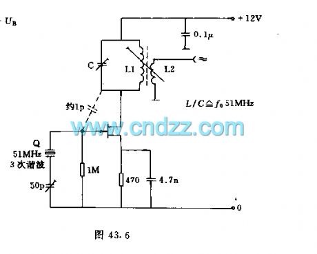
Crystal oscillator works as 51MHz crystal( the third harmonic of 17MHz) . According to the different structures, the drain - gate capacitance can be selected between 0.5 to 1.8 pF. L2's turns are about 20% of the L1. 470 Ω source resistor can change the oscillation characteristics.
(View)
View full Circuit Diagram | Comments | Reading(1930)
Fundamental Pierce oscillator circuit
Published:2012/8/12 22:29:00 Author:Ecco | Keyword: Fundamental Pierce , oscillator
The oscillator uses a fundamental quartz crystal, and the oscillation frequency can be up to 10MHz. Oscillator circuit is tuned to the resonant frequency. Capacitor C requires below 4.7pF, and it is connected to a follower to isolate the quartz crystal circuit.
(View)
View full Circuit Diagram | Comments | Reading(2366)
The quartz crystal oscillator circuit using NAND gate
Published:2012/8/12 22:31:00 Author:Ecco | Keyword: quartz crystal oscillator , NAND gate
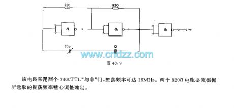
The circuit uses two 7400 TTL NAND gates, the oscillator frequency can reach 18MHz. Two 820 Ω resistors must be selected by oscillator frequency.
(View)
View full Circuit Diagram | Comments | Reading(2363)
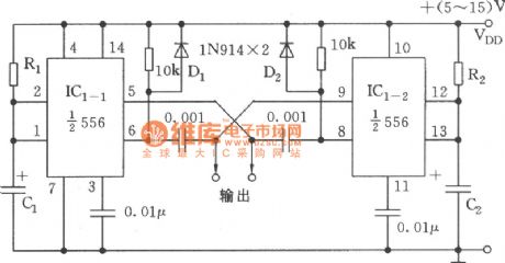
555 dual astable multivibrator circuit diagram
Published:2012/7/23 3:10:00 Author:Ecco | Keyword: 555, dual astable multivibrator


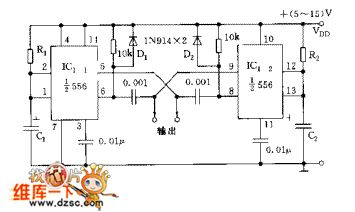
The circuit includes two synchronized multivibrators which are composed ofone pair of 555time base circuits. The circuit can output two synchronized pulse signals ,and the spacing and frequency can be changed by adjusting the time constant. The circuit is flexible and convenient.
When C1=C2=C, the oscillation frequency
The ducy cycle depends on the value of R1 and R2, and it can reach 5% ~ 95%.
(View)
View full Circuit Diagram | Comments | Reading(3558)
Stereo encoder circuit diagram with discrete components
Published:2012/7/16 2:53:00 Author:Ecco | Keyword: Stereo encoder , discrete components
View full Circuit Diagram | Comments | Reading(1199)
Bistable multivibrator circuit diagram
Published:2012/7/11 2:00:00 Author:Ecco | Keyword: Bistable multivibrator


As shown in the figure, the circuitaretwo synchronized multivibrators composed of composed of two dualtime-base circuits 556, and itcan output two synchronous clock pulse signals, and the spacing and oscillation frequency can be changed by adjusting the time constant. It isflexibleand convenient. When you select C1 = C2 = C3 , the oscillation frequency is
.
The duty cycle D depends on R1 and R2, which can reach 5%~95%.
(View)
View full Circuit Diagram | Comments | Reading(1979)
Closed-loop three-phase multivibrator oscillator circuit diagram
Published:2012/7/11 1:37:00 Author:Ecco | Keyword: Closed-loop, three-phase multivibrator

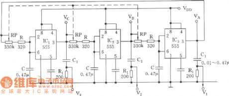
As shown in the figure,the closed loop is composed of three identical Schmitt triggers connnectedend to end. Each trigger's delay timetd = l . 1 (RP + R) C,and td is the time required by voltage on C to rise to 1/3 VDD. After 555 resets, the charge on C is dischared by formerIC output ( pin 3 ) through R, W, and thus the charging time constant is the same with C's. Once each trigger circuit's output endneeds to change, it requires to be transmitted three single stable trigger circuits, and the required time is 3td Therefore, the output cycle of each IC Td = 6td . The corresponding frequencyis
(View)
View full Circuit Diagram | Comments | Reading(3958)
Rf driver audio oscillator circuit diagram
Published:2012/7/11 1:22:00 Author:Ecco | Keyword: Rf driver, audio oscillator
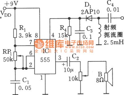
As shown in the figure, 555, Rl, RPland C1form thecontrolled audio oscillator , f = 1.44 / ( R1 +2 RP1) C1 , the icon parameter frequency isbetween 600Hz ~ 20kHz , and it can beselected by adjusting RP1.
(View)
View full Circuit Diagram | Comments | Reading(2193)
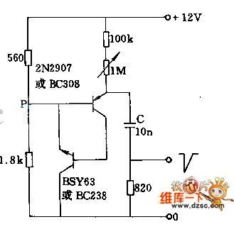
Synchronized clock oscillator circuit diagram
Published:2012/7/8 21:23:00 Author:Ecco | Keyword: Synchronized clock oscillator
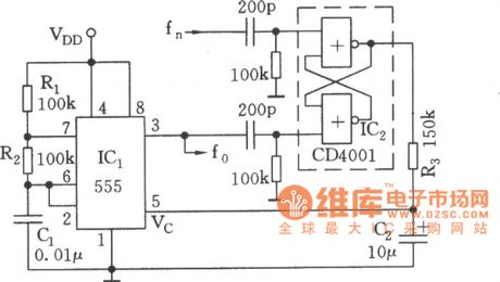
As shownin the figure, the controlled multivibrator iscomposed of 555 and R1, R2, C1, and the oscillation frequency is related to the RC time constant , but alsocan beadjustedby DC level of the control side. The DC level depends on the reference frequency f. After low-pass filter, the square wave is output by RS flip flop which is locked by oscillation frequency fo = Nfn output from 555. CD4001's two NOR gate circuits form the RS flip flop , when it is in a locked case , the duty cycle of the output will be kept, and thus the filtered DC level keepsconstant. If 555 oscillation frequency f0drift high(or fn reduces) , then the duty cycle will increase, thenthe DC control level will increase accordingly , frequency will decline; and vice versa.
(View)
View full Circuit Diagram | Comments | Reading(1728)
5kHz electric eye oscillation circuit
Published:2011/12/1 21:27:00 Author:May | Keyword: 5kHz, electric eye, oscillation
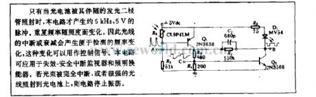
This circuit can generate 5kHz, 5V pulse only when electric eye is shined by its incidental LED. Repeat frequency changes along with illumination intensity. So the break off or weaken of optical line can generate frequency variation. This frequency variation is easy to detect. It can be usedfor controlling signal. This circuit can be applied to invalidation-safe interrupt monitor and illumination transducer. If the beam isinterrupted completely, or very strong optical line shines on electric eye, the circuit stops oscillation.
(View)
View full Circuit Diagram | Comments | Reading(1650)
VCT3802 CPU, VCD single chip small-signal process integrated circuit diagram
Published:2011/8/10 4:11:00 Author:Nicole | Keyword: single chip, small-signal process
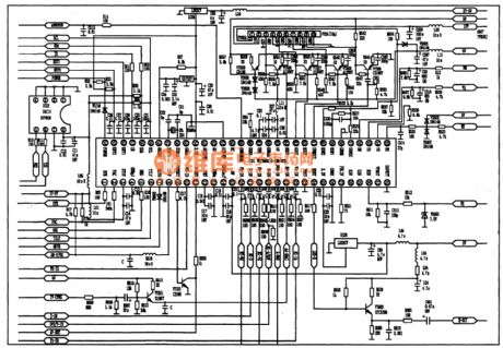
VCT3802 is a new type CPU, VCD single chip small-signal process integrated circuit which is used in multi-system color TV, it is widely used in new type large-screen color TV.
1, functions and features
The main functions of VCT3802 integrated circuit including: microprocessor, TV/AV switching circuit, brightness signal process circuit, color singal demodulator circuit, RGB matrix circuit, RGB singal selection switch circuit, adjusting-free line/field oscillation circuit and line/field pulse singal forming circuit, pincushion distort correcting signal process circuit and imaging state regulating circuit. The typical application circuit of this integrated block is shown in the figure 1-1.
The figure 1-1 is the typical application circuit of VCT3802 integrated block
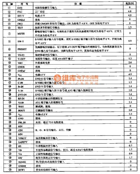
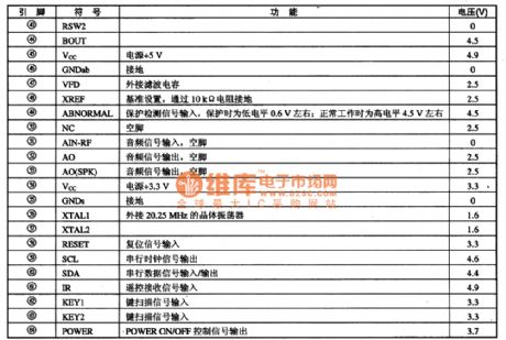
2, pin function and data
The pin function and data of VCT3802 integrated circuit is shown in the table 1-2
The table 1-2 is the pin function and data of VCT3802 integrated circuit (View)
View full Circuit Diagram | Comments | Reading(900)
Analog qigong infrared light generator circuit
Published:2011/11/9 21:25:00 Author:May | Keyword: Analog qigong , infrared light generator
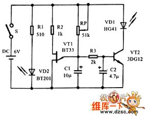
The following diagram is the principle diagram of Analog qigong infrared light generator circuit, andtransistor VT1 ect makes up unijunction pulse oscillator to generate about 10Hz STW, and it is filteredthrough R3, C2 and amplified byVT2 to drive infrared LED VD2 andgenerate pulse infrared light. PR is used for frequency vernier regulation, VD1 is the power source indication, VD2 is HG41domestic infrared LED, andits peak wavelength isgreater than 0.9μm, response time is smaller than 10ms.
Because qigong differs from man to man, and this generator only simulates outside gas information in some ways ( outside gas information is extremely rich) ,it allows component value to have wide change. HG41 isadded lens to makedivergence angle smaller than 20 degree, and its directivity is good. When people use it, peopel canput the infrared tube to aim at spontaneous in the palm or bellybelownavel hole, then it can generate sense of hotness after about 10 min. This generator can beused to qigong medical treatment or body stengthen experiment.
(View)
View full Circuit Diagram | Comments | Reading(1145)
Pulse generator circuit using two complementary transistors
Published:2011/10/31 1:58:00 Author:May | Keyword: Pulse generator , two complementary transistors
It usestwo complementary transistorsto produce pointed pulse with theamplitude in 8V, rise time in 50nS+. This circuit pulse intermission is 1.4ms at the situation of charging capacitance is 10nF and 1M potentiometershort-circuited, and the weakening or decreasing capacitance value can make the pulse intermission increase or decrease. If 820Ω resistor isconnected at the emitter of NPN transistor instead of series with capacitor, it will get sharp pulse output.
(View)
View full Circuit Diagram | Comments | Reading(4271)
Square-wave generator circuit
Published:2011/10/31 2:00:00 Author:May | Keyword: Square-wave generator
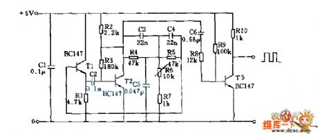
T1 and T2 in the circuitform theinherent oscillator, T3 is output level. Network consists of high-pass filter (C3, C4, R6 + - R7) and low pass filter, it's output is added to the T3 base via C6 and R8, and in the collector of T3, it willget required square wave oscillation signal.
(View)
View full Circuit Diagram | Comments | Reading(1994)
The square-wave generator circuit with variable pulse width
Published:2011/10/31 2:06:00 Author:May | Keyword: square-wave generator , variable pulse width
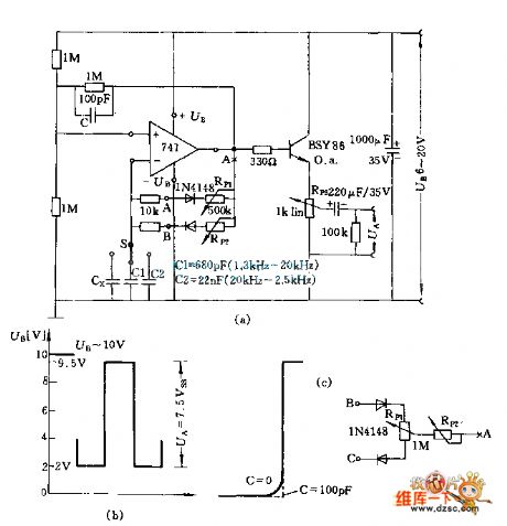
The circuit uses theswitch Sto change the output pulse frequency range (20HZ ~ 20KHZ). Potentiometer RP1, rP2 are not only used for changing frequency, also can used to change pulse width. If changing RP2, RP1at the same time, it will only change frequency, the pulse width approximate remains unchanged. If only changing one potentiometer, it can form asymmetric positive or negative square wave signal. Diagram (b) shows a typical wave.
If the circuitbetween A, B, C in the diagram is replaced by diagram (C) , it can use RP1 to change duty ratio, use RP2 to change frequency. Here RP1 chooses >1MΩ, RP2 chooses 1MΩ, then it can get positive and negative sharp pulse output in low frequency.
(View)
View full Circuit Diagram | Comments | Reading(1970)
Crystal oscillator circuit using operational amplifier
Published:2011/10/31 2:07:00 Author:May | Keyword: crystal oscillator, operational amplifier
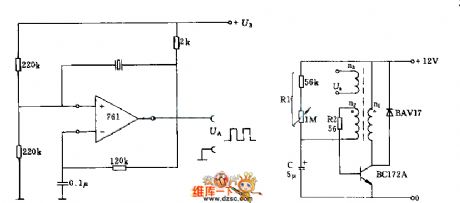
This circuit uses 761 operational amplifier, and theoutput pulse frequency can reach 10MHz. The 2KΩ resistor isused as operational amplifier output stage collector's load.
(View)
View full Circuit Diagram | Comments | Reading(2341)
The multivibrator circuit diagram with thyristor
Published:2011/10/31 2:14:00 Author:May | Keyword: multivibrator, thyristor
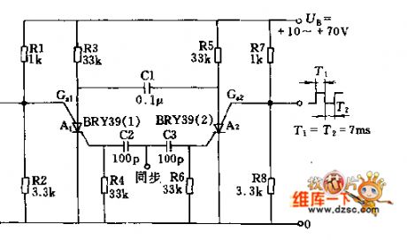
The circuit can produce 50V rectangular pulse, and its duty cycle T1 / (T1 + T2) canreach from 0.001 to 0.999 bycontinuously adjusting. This can be achieved by choosing the proper R3 and R5. Capacitor C1 and resistor R5can decide thefrequency, then the duty cycle is 50%.
(View)
View full Circuit Diagram | Comments | Reading(1698)
| Pages:41/195 At 204142434445464748495051525354555657585960Under 20 |
Circuit Categories
power supply circuit
Amplifier Circuit
Basic Circuit
LED and Light Circuit
Sensor Circuit
Signal Processing
Electrical Equipment Circuit
Control Circuit
Remote Control Circuit
A/D-D/A Converter Circuit
Audio Circuit
Measuring and Test Circuit
Communication Circuit
Computer-Related Circuit
555 Circuit
Automotive Circuit
Repairing Circuit