
A/D converter
Index 3
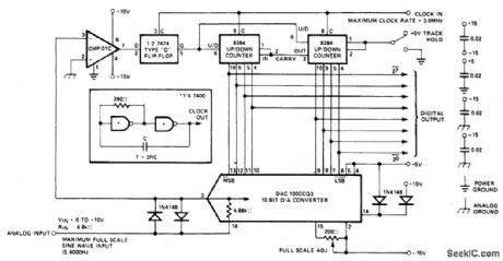
8_BIT_TRACKING_A_D_CONVERTER
Published:2009/6/24 1:41:00 Author:May
View full Circuit Diagram | Comments | Reading(920)
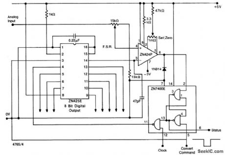
8_BIT_A_D_CONVERTER_1
Published:2009/6/24 1:39:00 Author:May
View full Circuit Diagram | Comments | Reading(1078)
SUCCESSIVE_APPROXIMATION_A_D_CONVERTER
Published:2009/6/24 1:36:00 Author:May
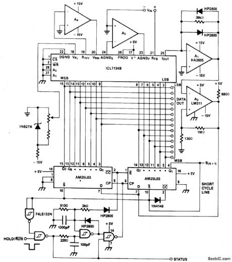
A bipolar input, high speed A/D converter uses two AM25L03s to form a 14-bit successive approximation register. The comparator is a two-stage circuit with an HA2605 front-end amplifier used to reduce settling time problems at the summing node. Careful offset-nulling of this amplifier is needed. (View)
View full Circuit Diagram | Comments | Reading(3)
8_BIT_A_D_CONVERTER
Published:2009/6/24 1:33:00 Author:May
View full Circuit Diagram | Comments | Reading(0)
BUFFER_FOR_A_D_CONVERTERS
Published:2009/6/22 22:47:00 Author:May
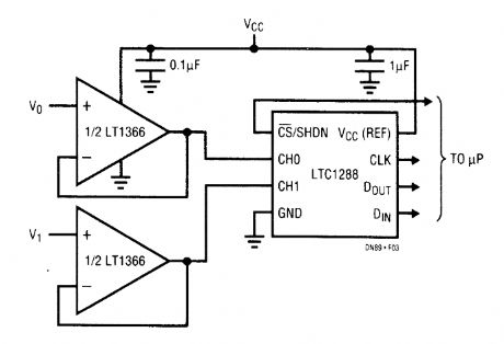
This circuit uses an LT1366 driving an LTC1288 two-channel micropower A/D. The LTC1288 can accommodate voltage references and input signals equal to the supply rails. The sampling nature of this A/D eliminates the need for an external sample-and-hold, but might call for a drive amplifier be-cause of the A/D's 12-ps settling requirement. The LT1366's rail-to-rail operation and low-input off-set voltage make it well suited for low-power, low-frequency A/D applications. In addition, the op-amp's output settles to 1% in response to a 3-mA load step through 100 pF in less than 1.5μs. (View)
View full Circuit Diagram | Comments | Reading(0)
A_D_CONVERTER_FOR_PCs
Published:2009/6/18 22:57:00 Author:May
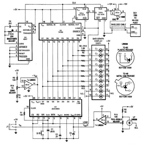
An ADC0804 A/D converter converts analog data to digital. This is fed ister and converted to serial data. U3 provides a baud-rate clock. U4A and start and stop bits needed at beginning and end of each data word. (View)
View full Circuit Diagram | Comments | Reading(3447)
HIGH_SPEED_A_D_CONVERTER_SYSTEM
Published:2009/6/18 22:54:00 Author:May
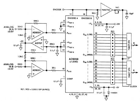
The AD8001 is well suited for driving high-speed analog-to-digital converters, such as the AD9058.The AD9058 is a dual 8-bit 50 Msps ADC. In the circuit shown, there are two AD8001s driving the in-puts of the AD905f8 which are configured for 0- to +2-V ranges. Bipolar input signals are buffered, amplified (-2x), and offset (by +1.0 V) into the proper input range of the ADC. Using the AD9058's internal +2-V reference connected to both ADCs (as shown) reduces the number of external com-ponents required to create a complete data acquisition system. The 20-Ω resistors in series with ADC input are used to help the AD8001 drive the 10-pf' ADO input capacitance. The two AD8001s only add 100 mW to the power consumption while not limiting the performance of the circuit. (View)
View full Circuit Diagram | Comments | Reading(1013)
8_CHANNEL_A_D_CONVERTER_FOR_PC_CLONESCont
Published:2009/6/15 4:18:00 Author:May
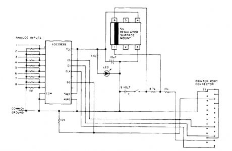
An A/D converter by National Semiconductor(ADC0838),converts 0- to 5-V analog inputs to adigital data format A 9-V battery is used.The converter connects to the pointer port connector viaa 25-pin connector (View)
View full Circuit Diagram | Comments | Reading(1637)
ADO_POLLER
Published:2009/6/15 4:15:00 Author:May
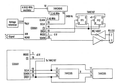
Because the CS5501 16-bit-delta-sigma analog-to-digital converter lacks a start convert com-mand, it converts continuously, outputting conversion words to its output register every 1024 cycles of its master clock. However, by incorporating a standard dual J-K flip-flop into the circuit, the ADC can be configured to output a single-conversion word only when it is polled.The CS5501 converter can be operated in its asynchronous communication mode (UART) to transmit one 16-bit conversion word when it is polled over an RS-232 serial line (see figure). A null character (all zeros) is transmitted to the circuit and sets the flip-flop FE2. The CS5501 can then out-put a single-conversion word, which is transmitted over the RS-232 line as two bytes with start and stop bits.The baud rate can be chosen by selecting the appropriate clock divider rate on the 74HC4040 counter/divider as the serial port clock (SLCK) for the ADC. This type of polled-mode operation is also useful when the ADC's output register is configured to operate in the synchronous-serial clock (SSC) mode. In this case, the converter will load one output word into a 16-bit serial-to-parallel reg-ister (two 74HC595 8-bit registers) when polled to do so (see figure). (View)
View full Circuit Diagram | Comments | Reading(1344)
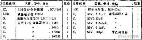
Low-power liquid crystal display 3 1/2 A-D converter circuit
Published:2011/6/3 20:53:00 Author:Fiona | Keyword: Low-power liquid crystal display
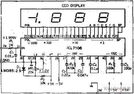
Circuit function
This is a digital display type A-D converter.It is suitable for portable small measuring instrument. Because of the use of liquid crystal display andLow consumption, Full range display voltage is 1.999V. If the input voltage is greater than this value, it should be added a attenuator.The circuit is more used for measuring instrument.Its power source voltage is in positive and negative 5V.
Circuit Work
3 1 / 2-bit A-D converter ICL7106 is a monolithic LSI that can directly drive liquid crystal display, is general Instrument IC and other companies have processed products. A - D convert way is ordinary double integral type, differential input circuit can input positive and negative about 1V phase voltage, the internal does automatic zero set. Circuit adjustment can only use VR1.
(View)
View full Circuit Diagram | Comments | Reading(2467)
formed by common components 4 input 12-bit A-D converter diagram
Published:2011/5/11 3:23:00 Author:Fiona | Keyword: formed by common components, 4 input
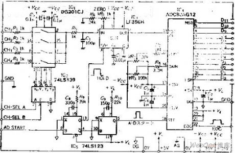
Circuit function
Recently, there is a variety of general-purpose AD conversion expansion board as a personal computer expanded with being sold on the market , if limited specific use, production costs can be low.
This circuit is a 12-bit AD converterusing in sample and hold circuits which is composed of the universal element and 4 inputs. It can enter positive and negative analog signals.
Circuit work
Analog input mux using the standard analog switch DG201, chooses 1~4 channel with decoder IC , channel selection input control by the two positive logic. After selecting channel, input about 10US wide sampling pulse to the sample and hold circuit to keep the analog voltage.The pulse starts to pulse by the AD pulse, using the pulse rising edge to begin 12-bit conversion. The conversion time is about 25US, 12-bit data output from D0 ~ D11. About EOC signal: when A-D conversion starts, EOC is H level and count the clock pulse.After conversion, EOC is back L level, so we can use the method of detecting EOC signai's rising and falling to read the slide 12-bit data.
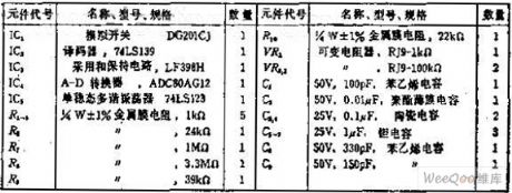
Component selection
(View)
View full Circuit Diagram | Comments | Reading(824)
| Pages:3/3 123 |
Circuit Categories
power supply circuit
Amplifier Circuit
Basic Circuit
LED and Light Circuit
Sensor Circuit
Signal Processing
Electrical Equipment Circuit
Control Circuit
Remote Control Circuit
A/D-D/A Converter Circuit
Audio Circuit
Measuring and Test Circuit
Communication Circuit
Computer-Related Circuit
555 Circuit
Automotive Circuit
Repairing Circuit