
A/D converter
Index
12-bit A / D conversion system circuit of AD585
Published:2013/1/30 1:43:00 Author:Ecco | Keyword: 12-bit , A / D conversion system
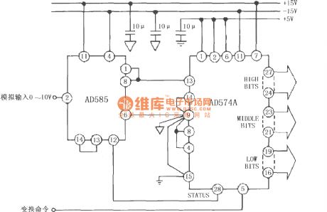
AD585 has a fast sampling time, therefore it can be applied to multi-channel data acquisition system, and it can complete the A / D conversion with high-frequency signal and high passing rate.
(View)
View full Circuit Diagram | Comments | Reading(1633)
Video speed 6-bit Flash A/D converter
Published:2012/9/12 21:00:00 Author:Ecco | Keyword: Video speed , 6-bit, Flash, A/D converter
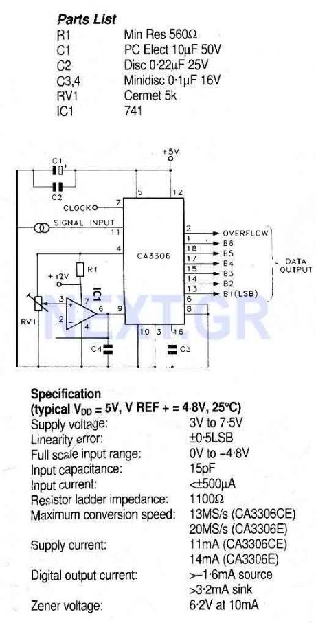
This circuit use the CA3306 a family of CMOS parallel (flash) analogue to digital converters designed for low power, high speed applications. The CA3306CE operates at sampling rates up to 10 million samples per second and the CA3306E up to 15 million samples per second permitting analogue signals with bandwidths up to 5MHz or 7.5MHz to be fully digitised to 6-bit accuracy.
Source: NEXT.GR (View)
View full Circuit Diagram | Comments | Reading(1374)
Analogue to digital converter circuit
Published:2012/9/11 21:19:00 Author:Ecco | Keyword: Analogue to digital, converter
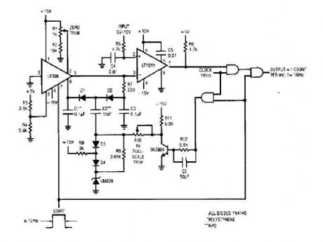
That simple 4 digits converter circuit has OUTPUT COUNT = 1 according to my f-IMHz to 10.000. All diodes are IN4146 POLYSTYRENE NPO. (View)
View full Circuit Diagram | Comments | Reading(3840)
16 bit Analogue to Digital Converter LTC1052
Published:2012/9/11 21:18:00 Author:Ecco | Keyword: 16 bit, Analogue to Digital , Converter
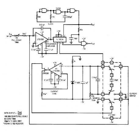
The circuit here is a A/D converter, that consisting of A2, a flip-flop, some doors and a current sink, is based on a current balancing technique. Again, the stabilized LTC 1052 50 no drift of V input 1 ° C is necessary to eliminate the offset errors of aid. (View)
View full Circuit Diagram | Comments | Reading(1829)
10 Bit A-D converter circuit
Published:2012/9/11 21:18:00 Author:Ecco | Keyword: 10 Bit , A-D converter
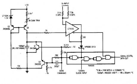
Each time a pulse is applied to the conversion of the control input, Ql resets the 1000 pF capacitor to 0 V. This action takes 200 ns to reset the falling edge of the convert command pulse, the capacitor begins to charge linearly. In exactly 10 microseconds, it loads to 2.5 V. The ramp is 10 microseconds applied to the positive input of the LTl016. The LT1016 compares the ramp Ex, the unknown, its negative input. For a 0 V - 2.5 V range, Ex is applied to the resistance of 2.5 k ohm. (View)
View full Circuit Diagram | Comments | Reading(1630)
A/D Converter with LT1018
Published:2012/9/11 21:18:00 Author:Ecco | Keyword: A/D Converter
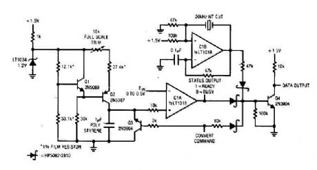
The converter has a 60-ms conversion consumes 460 pA of 1's. 5 V power supply and maintains an accuracy of 10 bits on a 15 ° C in the temperature range of 35 ° C. A pulse applied to convert the command line causes Q3, operating in reverse mode, the discharge path through the diode 10 kO, forcing its collector low. Q3 results of reverse mode switching in a capacitor discharge to 1 mV of ground. During the time of the ramp value is less than the input voltage, output of the CIA is low. (View)
View full Circuit Diagram | Comments | Reading(1494)
High Speed A/D converter 12-bit
Published:2012/9/11 21:17:00 Author:Ecco | Keyword: High Speed , A/D converter, 12-bit
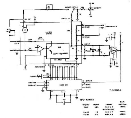
This system performs a complete conversion of 12 bits in 10 p unipolar or bipolar. This converter is accurate to ± 12-bit LSB Y2 and a typical gain TC of 10 ppm / ° C. In unipolar mode, the system range is 0 V to 9.9976 V, with each bit having a value of 2.44 mY. For the accuracy of true conversion, an A / D converter must be trimmed so that, given the results just the exit code of input levels of Y2 Y2 LSB LSB below to above the exact voltage represents the code. (View)
View full Circuit Diagram | Comments | Reading(1409)
Simple A/D converter circuit with 2504
Published:2012/9/11 21:16:00 Author:Ecco | Keyword: Simple A/D converter
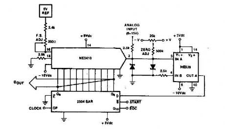
Time IO-bit conversion is 3.3 MHz with a p 3. Clock. This converter uses an approximation 2504 12-bit register in successive operating mode where the short-cycle end signal conversion is taken from the first bit used in the SAR (QLO). (View)
View full Circuit Diagram | Comments | Reading(1127)
14 Bit A-D Converter with ICL7134B
Published:2012/9/11 21:16:00 Author:Ecco | Keyword: 14 Bit , A-D Converter
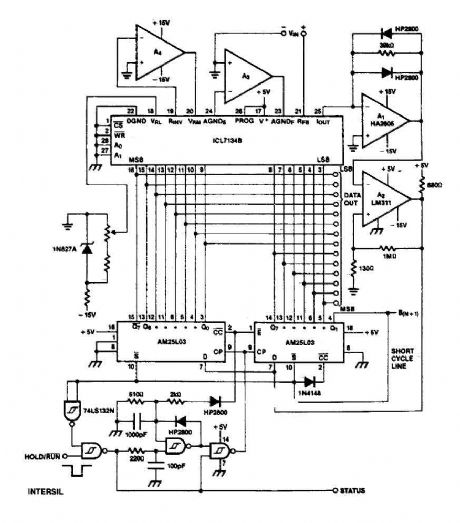
The circuit ICL7134B base is a bipolar input AID converter broadband, using two AM25L03s to form a successive approximation register 14-bit. The comparator is a circuit with two stage amplifier HA2605 front, used to reduce the settling time problems in the pro summing node (see A020). Warning nu11ing offset of this amplifier is needed and if wide temperature range operation is desired, an auto-zero circuit using a lCL7650 is probably desirable (see A053). The clock, using two gates TTL Schmitt trigger operates at a slower pace for the first 8 bits, where the settlement time is more critical than for the last 6 bits. (View)
View full Circuit Diagram | Comments | Reading(1486)
Cyclic A/D converter circuit
Published:2012/9/11 21:15:00 Author:Ecco | Keyword: Cyclic A/D converter
The cyclic converter consists of a chain of identical stages, each of which detects the polarity of the input. Step V REF then subtracted from the double entry and the rest if the polarity is correct. The signal is full wave rectified and the rest of V IN - V REF is doubled. (View)
View full Circuit Diagram | Comments | Reading(1043)
Differential A/D Converter circuit CA3110
Published:2012/9/11 21:15:00 Author:Ecco | Keyword: Differential, A/D Converter
By using an op amp BiMOS CA3140 provides good orientation skills for high bandwidth signal input, and can quickly adjust the energy output at its terminal CA33IO WINE. The CA3140 can also lead to near the negative supply rail. (View)
View full Circuit Diagram | Comments | Reading(1693)
COMPUTER_CONTROLLED_A_D_CONVERTER
Published:2009/7/12 22:18:00 Author:May
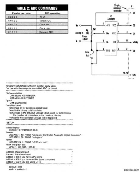
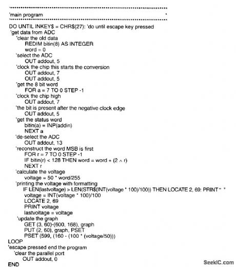
This simple, inexpensive computer-controlled A/D converter (ADC) plugs into a PC parallel port. The 8-bit peripheral device requires only seven components controlled to imponents and is imkplement and is completely controllde by a short BASIC program. (View)
View full Circuit Diagram | Comments | Reading(1146)
ANALOG_DIGITAL_CONVERSION
Published:2009/7/5 22:09:00 Author:May

Circuit canbe used for either ramp orsuccessive-approximation method of converting analog input to digital word, applying it to DAC, and comparing analog output of DAC to analog input to be converted. Results of comparison determine next digital word to be generated for DAC by microprocessor. LM301A changes 0-2 mA output of DAC into 0-5 V for LM311 comparator. To calibrate, apply all 0s to DAC; pin 6 of LM301A should now be near 0V Apply all 1s to DAC and adjust output of LM301A to 5.00 V with R4,Conversion routines implementing these functions are given for Motorola MC6800 and Intel 8008 microprocessors.-R, Frank, Microprocessor Based Analog/Digital Conversion.BYTE, May 1976.p70-73. (View)
View full Circuit Diagram | Comments | Reading(1989)
HALF_FLASH_ADC
Published:2009/7/5 21:17:00 Author:May
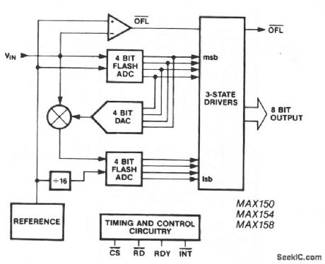


An a/d conversion technique which combines some of the speed advantages of flash conversion with the circuitry savings of successive approximation is termed half-flash. In an 8-bit, half-flash converter, two 4-bit flash a/d sections are combined. The upper flash a/d compares the input signal to the reference and generates the upper 4 data bits. This data goes to an internal DAC, whose output is subtracted from the analog input. Then, the difference can be measured by the second flash a/d, which provides the lower 4 data bits. (View)
View full Circuit Diagram | Comments | Reading(2628)
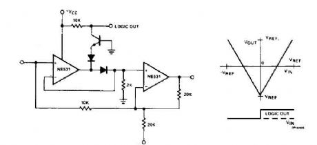
ADC
Published:2009/7/5 21:10:00 Author:May
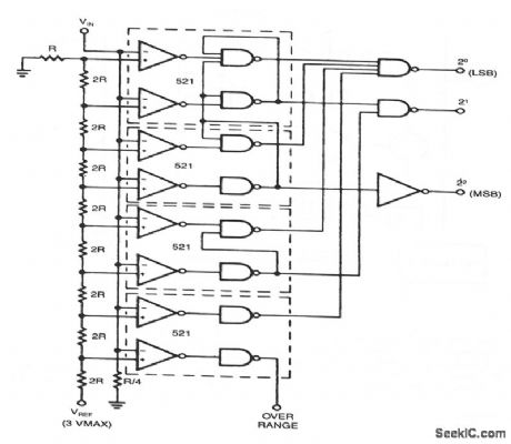
Conversion speed of this design is the sum of the delay through the comparator and the decoding gates. Reference voltages for each bit are developed from a precision resistor ladder network. Values of R and 2R are chosen so that the threshold is 1/2 of the least significant bit. This assures maximum accuracy of ±1/2 bit. The individual strobe line and duality features of the NE521 greatly reduced the cost and complexity of the design. (View)
View full Circuit Diagram | Comments | Reading(2935)
TRACKING_ADC
Published:2009/7/5 21:08:00 Author:May
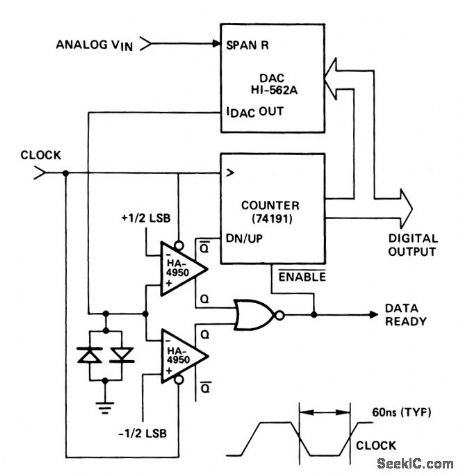
The analog input is fed into the span resistor of a DAC .he analog input voltage range is selectable in the same way as the output voltage range of the DAC.The net current flow through the ladder termination resistance;i.e.,2 KΩ for HI-562A; produces an error voltage at the DAC output.This error voltage is compared with 1/2 LSB by a comparator. When the error voltage IS within±1/2 LSB range,the Q output ofthe comparators are both low,which Stops the counter and gives a data ready signal to indicate that the digital output is correct,If the error exceeds the±1/2 LSB range,the counter iS enabled and driven In anup or down direction depending on the polarity of the error voltage.
The digital output changes state only when there is a significant change in the analog input.When monitoring a slowly varying input,it is necessary to read the digital output only after a change has taken place.The data ready signal could be used to tngger a flip-flop to indicate the condition and reset it after readout.The main disadvantage of the tracking ADC iS the time required to initially acqutre a signal;for a 12-bit ADC,it could be up to 4096 clock periods.The input signal usually must be filtered so that its rate of change does not exceed the tracking range of the ADC—1 LSB per clock period.
(View)
View full Circuit Diagram | Comments | Reading(2025)
SWITCHED_CAPACITOR_ADC
Published:2009/7/5 20:57:00 Author:May
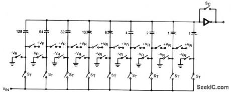
The CMOS comparator in the successive-approximation system determines each bit by examining the charge on a series of binary-weighted capacitors. In the first phase of the conversion process, the analog input is sampled by closing switch SC and all ST switches, and by simultaneously charging all the capacitors to the input voltage.
In the next phase of the conversion process, all ST and SC switches are opened and the comparator begins identifying bits by identifying the charge on each capacitor relative to the reference voltage. In the switching sequence, all 8 capacitors are examined separately until all 8 bits are identified, and then the charge-convert sequence is repeated. In the first step of the conversion phase, the comparator looks at the first capacitor (binary weight = 128). One pole of the capacitor is switched to the reference voltage, and the equivalent poles of all the other capacitors on the ladder are switched to ground. If the voltage at the summing node is greater than the trip point of the comparator-approximately 1/2 the reference voltage, a bit is placed in the output register, and the 128-weight capacitor is switched to ground. If the voltage at the summing node is less than the trip point of the comparator, this 128-weight capacitor remains connected to the reference input through the remainder of the capacitor-sampling (bit-counting) process. The process is repeated for the 64-weight capacitor, the 32-weight capacitor, and so forth down the line, until all bits are tested. With each step of the capacitor-sampling process, the initial charge is redistributed among the capacitors. The conversion process is successive-approximation, but relies on charge shifting rather than a successive-approximation register-and reference d/a-to count and weigh the bits from MSB to LSB.
(View)
View full Circuit Diagram | Comments | Reading(1306)
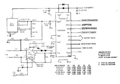
DIFFERENTIAL_INPUT_A_D_SYSTEM
Published:2009/7/2 4:06:00 Author:May
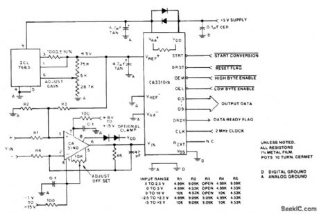
Using a CA3140 BiMOS op amp provides good slewing capability for high bandwidth input signals, and can quickly settle energy that the CA3310 outputs at its VIN terminal. The CA3140 can also drive close to the negative supply rail. If system supply sequencing or an unknown input voltage is likely to cause the op amp to drive above the VDD supply, a diode clamp can be added from pin 8 of the op amp to the VDD supply. (View)
View full Circuit Diagram | Comments | Reading(1171)
CYCLIC_A_D_CONVERTER
Published:2009/7/2 4:04:00 Author:May
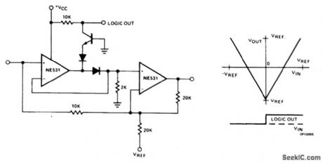
The cydic converter consists of a chain of identical stages, each of which senses the polarity of the input. The stage then subtracts VREF from the input and doubles the remainder if the polarity was correct. The signal is full-wave rectifted and the remainder of VIN - VREF is doubled. A chain of these stages gives the gray code equivalent of the input voltage in digitized form related to the magnitude of VREF. Possessing high potential accuracy, the circuit using NE531 devices settles in 5 μs. (View)
View full Circuit Diagram | Comments | Reading(1036)
SUCCESSIVE_APPROXIMATION_A_D_CONVERTER_1
Published:2009/7/2 4:02:00 Author:May
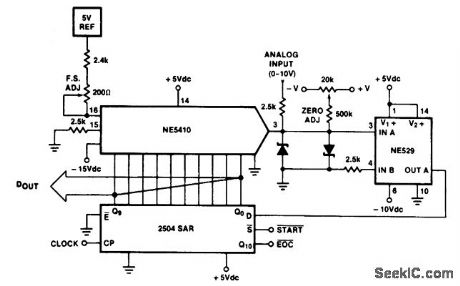
The 10-bit conversion time is 3.3 μs with a 3 MHz clock. This converter uses a 2504 12-bit successive approximation register in the short cycle operating mode where the end of conversion signal is taken from the first unused bit of the SAR (Q10). (View)
View full Circuit Diagram | Comments | Reading(1151)
| Pages:1/3 123 |
Circuit Categories
power supply circuit
Amplifier Circuit
Basic Circuit
LED and Light Circuit
Sensor Circuit
Signal Processing
Electrical Equipment Circuit
Control Circuit
Remote Control Circuit
A/D-D/A Converter Circuit
Audio Circuit
Measuring and Test Circuit
Communication Circuit
Computer-Related Circuit
555 Circuit
Automotive Circuit
Repairing Circuit