
A/D converter
Index 2
HIGH_SPEED_12_BIT_A_D_CONVERTER
Published:2009/7/2 4:00:00 Author:May
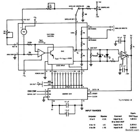
This system completes a full 12-bit conversion in 10 μs unipolar or bipolar. This converter will 6e accurate to ±1/2 LSB of 12 bits and have a typical gain TC of 10 ppm/℃. In the unipolar mode, the system range is 0 V to 9.9976 V, with each bit having a value of 2.44 mV. For the true conversion accuracy, an A/D converter should be trimmed so that given bit code output results from input levels from 1/2 LSB below to 1/2 LSB above the exact voltage which that code represents. Therefore, the converter zero point should be trimmed with an input voltage of 1.22 mV; trim R1 until the LSB just begins to appear in the output code (all other bits 0 ). For full-scale, use an input voltage of 9.9963 V (10 V-1 LSB-1/2 LSB); then trim R2 until the LSB just begins to appear (all other bits 1 ). The bipolar signal range is -5.0 V to 4.9976 V. Bipolar offset trimming is done by applying a -4.9988 V input signal and trimming R3 for the LSB transition (all other bits 0 ). Full-scale is set by applying 4.9963 V and trimming R2 for the LSB transition (all other bits 1 ). (View)
View full Circuit Diagram | Comments | Reading(1304)
10-BIT_A_D_CONVERTER
Published:2009/7/2 3:56:00 Author:May
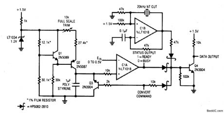

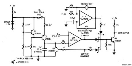
The converter has a 60 ms conversion time, consumes 460 μA from its 1.5 V supply and maintains 10 bit accuracy over a 15℃ to 35℃ temperature range. A pulse applied to the convert command line causes Q3, operating in inverted mode, to discharge through the 10 kΩ diode path, forcing its collector low. Q3's inverted mode switching results in a capacitor discharge within 1 mV of ground. During the time the ramps' value is below the input voltage, CIA's output is low. This allows pulses from C1B, a quartz stabilized oscillator, to modulate Q4. Output data appears at Q4's collector. When the ramp crosses the input voltages value C1A's output goes high, biasing Q4 and output data ceases. The number of pulses at the output is directly proportional to the input voltage. To calibrate apply 0.5 V to the input and trim the 10 kΩ potentiometer for exactly 1000 pulses out each time the convert command line is pulsed. (View)
View full Circuit Diagram | Comments | Reading(1248)
INEXPENSIVE,FAST_10_BIT_SERIAL_OUTPUT_A_D
Published:2009/7/2 3:53:00 Author:May
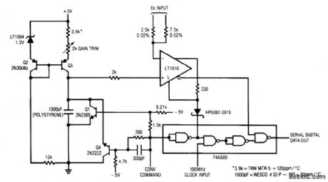
Everytime a pulse is applied to the convert command input, Q1 resets the 1000 pF capacitor to.0 V. This resetting action takes 200 ns of the falling edge of the convert command pulse, the capacitor begins to charge linearly. In precisely 10 microseconds, it charges to 2.5 V. The 10 microseconds ramp is applied to the LT1016's positive input. The LT1016 compares the ramp to Ex, the unknown, at its negative input. For a 0 V - 2.5 V range, Ex is applied to the 2.5 k ohm resistor. From a 0 V - 10 V range, the 2.5 k ohm resistor is grounded and Ex is applied to the 7.5 k ohm resistor. Output of the LT1016 is a pulse whose width is directly dependent on the value of Ex. This pulse width is used to gate a 100 MHz clock. The 100 MHz clock pulse bursts that appear at the output are proportional to Ex. For a 0 V - 10 V input, 1024 pulses appear at fullscale, 512 at 5.00 V, etc. (View)
View full Circuit Diagram | Comments | Reading(957)
16_BIT_A_D_CONVERTER
Published:2009/7/2 3:50:00 Author:May
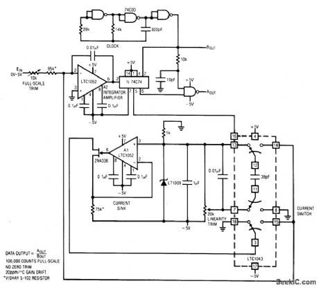
The A/D converter, made up of A2, a flip-flop, some gates and a current sink, is based on a current balancing technique. Once again, the chopper-stabilized LTC1052's 50 nV/℃ input drift is required to eliminate offset errors in the A/D. (View)
View full Circuit Diagram | Comments | Reading(1212)
4_DIGIT(10000_COUNT)A_D_CONVERTER
Published:2009/7/2 3:46:00 Author:May
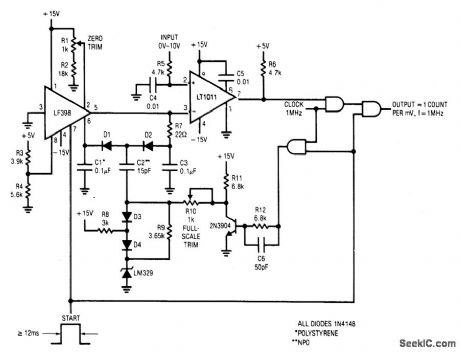
View full Circuit Diagram | Comments | Reading(1026)
SUCCESSIVE_APPROXIMATION_A_D_CONVERTERS
Published:2009/7/2 3:42:00 Author:May
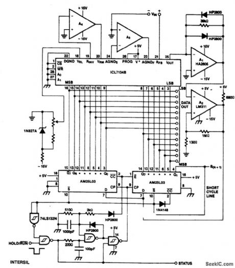
The ICL7134B-based circuit is for a bipolar-input high-speed A/D converter, using two AM25L03s to form a 14-bit successive approximation register. The comparator is a two-stage circuit with an HA2605 front-end amplifier, used to reduce settling time problerns at the summing node (see A020). Careful offset-nulling of this amplifier is needed, and if wide temperature range operation is desired, an auto-null circuit using an ICL7650 is probably advisable (see A053). The clock, using two Schmitt trigger TTL gates, runs at a slower rate for the first 8 bits, where settling-time is most critical than for the last 6 bits. The short-cycle line is shown tied to the 15th bit; if fewer bits are required, it can be moved up accordingly. The circuit will free-run if the HOLD/RUN input is held low, but will stop after completing a conversion if the pin is high at that time. A lowgoing pulse will restart it. The STATUS output indicates when the device is operating, and the falling edge indicates the availability of new data. A unipolar version can be constructed by typing the MSB (D13) on an ICL7134U to pin 14 on the first AM25L03, deleting the reference inversion amplifier A4, and tying VRFM to VRFL. (View)
View full Circuit Diagram | Comments | Reading(2066)
12_BIT_DAC_WITH_VARIABLE_STEP_SIZE
Published:2009/7/1 21:31:00 Author:May
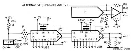
The step size of the converter is variable by selection of the high order data bits.The first DAC, A, has a stable reference current supplied via the 10.24 V reference IC and R1. R2 provides bias cancellation. As shown, only the first 4 MSB inputs are used, giving a step size of225/256 x 2.048/16 = 0.127 mA. This current supplies the reference for DAC B whose step size is then 0.1275/256 = 0.498 μA. Complementary voltage outputs are available for unipolar output and using R3 = R4 = 10 K, Vout is ±10.2 V pproximately, with a step size (1 LSB) of approximately 5 mV. If desired an op amp can be added to the output to provide a low impedance output with bipolar output symmetrical about ground, if R5 = R6 within 0.05%. Note that offset null is required, and all resistors except R2 and R3 should be 1% high stability types.By using lower order address lines than illustrated for DAC A, a smaller step size (and therefore full-scale output) can be obtained. Unused high order bits can be manipulated high or low to change the relative position of the full-scale output. (View)
View full Circuit Diagram | Comments | Reading(1061)
4_BIT_CLOCKLESS
Published:2009/6/30 1:56:00 Author:May

Simple and low-cost arrangement of seven CA3130 opamps gives conversion times fast enough for tracking sinewave signals well up into audio range, Even with relatively slow 741 opamps, signals up to 300 Hz were easily tracked. Additional bits are easily cascaded.—B. P. Vandenberg, Tracking-Type A/D Requires No Clock Oscillator, EDN Magazine, Jan. 20, 1977, p 92 and 94. (View)
View full Circuit Diagram | Comments | Reading(1193)
COMPRESSING_A_D_CONVERSION
Published:2009/6/30 1:50:00 Author:May
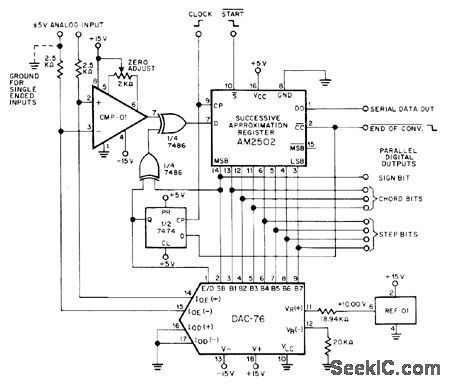
Step size increases as output changes from zero scale to full scale, in contrast to conventional linear converter in which step size is constant percentage of full scale. Uses Precision MonolithIcs DAC-76 D/A converter in combination with CMP-01 comparator, any standard EXCLUSIVE-OR gate, and successive-approximation register for conversion logic. Encoding sequence begins with sign-bit comparison and decision. Bits are con verted with successive-removal technique, starting with decision at code 011 1111 and turning off bits sequentially until all decisions have been made. Conversion is completed in nine clock cycles.— COMDAC Companding D/A Converter, Precision MonolithIcs, Santa Clara, CA, 1977, DAC-76, p 12. (View)
View full Circuit Diagram | Comments | Reading(1253)
HIGH_SPEED_SUCCESSIVE_APPROXIMATION
Published:2009/6/30 1:46:00 Author:May

Total converslon time for 8-bit system is about 4.5 μs,clock rate is up to 2 MHz. Serial output is used for transmission to one or more other location. —T. Henry, Successive Approximation A/D Conversion, Motorola, Phoenix, AZ, 1974, AN-716, p 5. (View)
View full Circuit Diagram | Comments | Reading(1455)
FOUR_CHANNEL_INPUT_MULTlPLEXING
Published:2009/6/30 1:40:00 Author:May
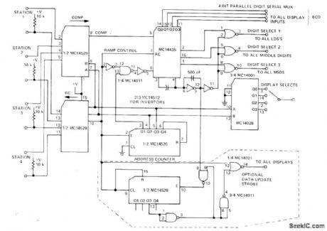
Conversion process is divided between central station and remote locations having analog sensors. Each station transmits two noise-immune low-frequency digital signals under control of central multiplexor. System is much more economical than having separate A/D converter at each sensor. Can be extended to 32 channels. Multiplexing is performed under control of clock in Motorola MC14435, operating between 100 kHz and 1 MHz. At 500 kHz, each conversion takes about 15 ms.—S. Kelley, Analog Data Acquisition Network for Digital Processino Using the MC1405-MC14435 A/D System, Motorola, Phoenix, AZ, 1975, EB-58. (View)
View full Circuit Diagram | Comments | Reading(1248)
EIGHT_INPUT_A_D_CONVERTER_FOR_TEMPERATURE_MEASUREMENTS
Published:2009/6/24 4:03:00 Author:May
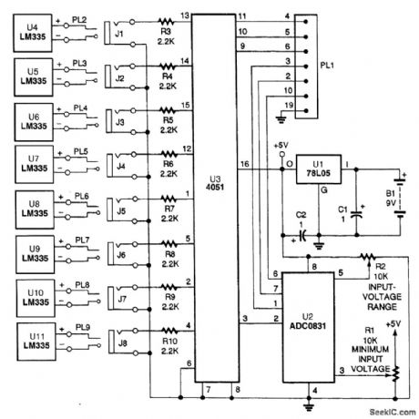

The actual processing circuitry of this A/D converter consists of only four parts: U2, U3, R1 and R2. Eight temperature probes are used with the circuit; however, they can be replaced with other types of sensors, as long as resistors R3 through R10 are removed.
(View)
View full Circuit Diagram | Comments | Reading(0)
THREE_IC_LOW_COST_A_D_CONVERTER
Published:2009/6/24 1:57:00 Author:May
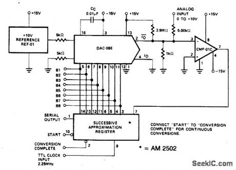
View full Circuit Diagram | Comments | Reading(938)
HIGH_SPEED_3_BIT_A_D_CONVERTER
Published:2009/6/24 1:55:00 Author:May
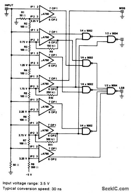
View full Circuit Diagram | Comments | Reading(1181)
FAST_PRECISION_A_D_CONVERTER
Published:2009/6/24 1:53:00 Author:May
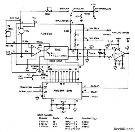
View full Circuit Diagram | Comments | Reading(835)
3_1_2_DIGIT_A_D_CONVERTER_WITH_LCD_DISPLAY
Published:2009/6/24 1:52:00 Author:May
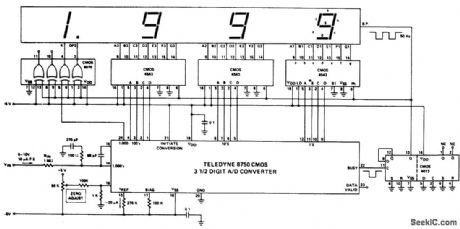
View full Circuit Diagram | Comments | Reading(1267)
TRACKING_SERVO_TYPE_A_D_CONVERTER
Published:2009/6/24 1:48:00 Author:May
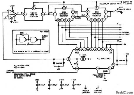
View full Circuit Diagram | Comments | Reading(889)
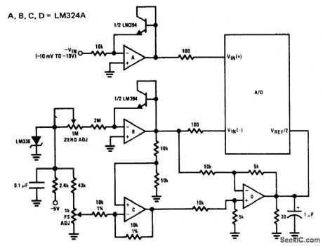
THREE_DECADE_LOGARITHMIC_A_D_CONVERTER
Published:2009/6/24 1:47:00 Author:May
View full Circuit Diagram | Comments | Reading(1180)
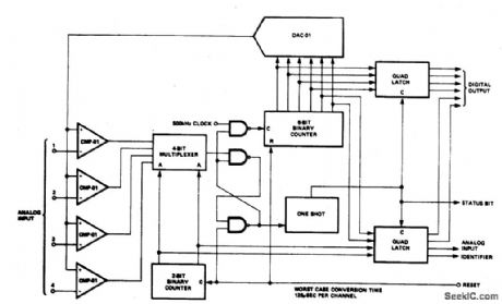
FOUR_CHANNEL_DIGITALLY_MULTIPLEXED_RAMP_A_D_CONVERTER
Published:2009/6/24 1:43:00 Author:May
View full Circuit Diagram | Comments | Reading(848)
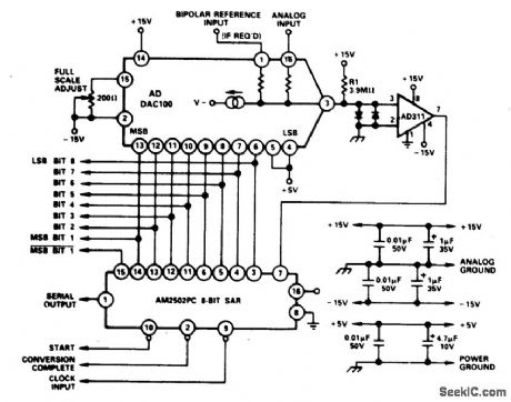
8_BIT_SUCCESSIVE_APPROXIMATION_A_D_CONVERTER
Published:2009/6/24 1:42:00 Author:May
View full Circuit Diagram | Comments | Reading(1)
| Pages:2/3 123 |
Circuit Categories
power supply circuit
Amplifier Circuit
Basic Circuit
LED and Light Circuit
Sensor Circuit
Signal Processing
Electrical Equipment Circuit
Control Circuit
Remote Control Circuit
A/D-D/A Converter Circuit
Audio Circuit
Measuring and Test Circuit
Communication Circuit
Computer-Related Circuit
555 Circuit
Automotive Circuit
Repairing Circuit