
Amplifier Circuits-Miscellaneous
Index
Deep-current negative feedback differential motion amplifier diagram
Published:2011/9/7 4:19:00 Author:Vicky | Keyword: deep-current, negative feedback, differential motion amplifier
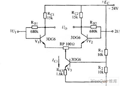
Deep-current negative feedback differential motion amplifier diagram
(View)
View full Circuit Diagram | Comments | Reading(967)
100KHz –100 MHz Noise Elimination Circuit Diagram
Published:2011/9/6 21:18:00 Author:Vicky | Keyword: noise elimination circuit
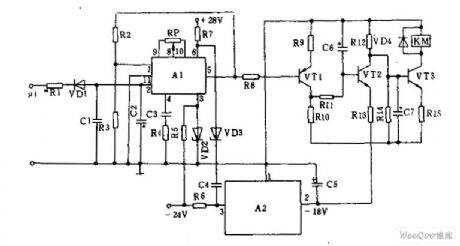
Noise elimination circuit can be designed in the 100kHz~l00MHz superhigh circuit. It is mainly composed by squelch amplifier AL, control circuit VTl~VT3, relay KNf, and regulated voltage supply A2. The working principle is shown in the above picture. When there is no signal received, the output noise voltage of superhigh frequency is lower than 100MV; the DC voltage of detection wave is very small after being filtered by diode VD1 and capacitances C1 and C2. The voltage enters the integrated amplifier A1via pin ② in the output end , and leaves via @. The voltage remains very small after amplified and cannot drive the triode VT1 to work. VT2 stops working and VT3 is under conducted. Relay KM then works.
(View)
View full Circuit Diagram | Comments | Reading(1289)
PARALLEL_LOOP_ALARM
Published:2009/6/14 21:39:00 Author:jailer
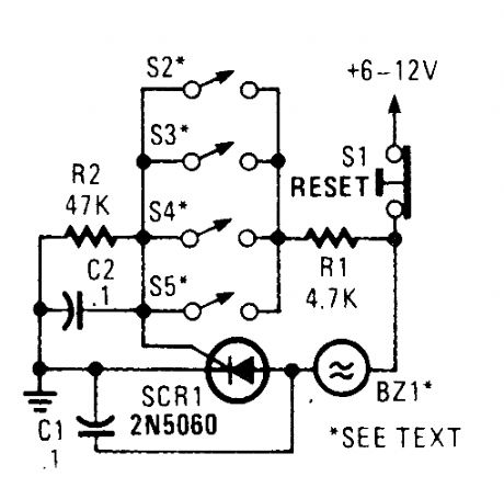
Four paraJlel switches are used to monitor four positions. When a closure occurs on any switch, SCR1 triggers, which sounds the alarm.The alarm should be of the noninterrupting type. (View)
View full Circuit Diagram | Comments | Reading(743)
The rotate speed test circuit made by optoelectronic transistor
Published:2011/7/13 20:10:00 Author:leo | Keyword: Rotate speed test circuit, Optoelectronic transistor
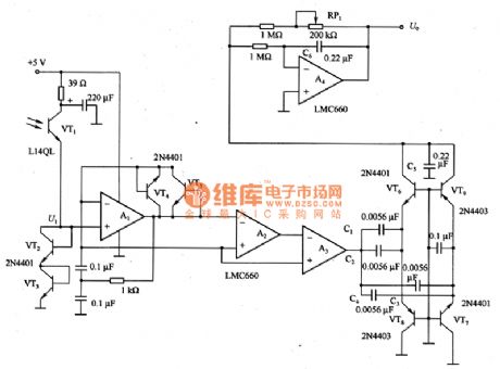
The picture1 shows rotate speed test circuit made by optoelectronic transistor and so on. When the luminous flux of the optoelectronic transistor VT1 increases by 1%, photo current generates 500 mV voltage between VT2 and VT3. And this voltage is stable logarithm relation under the biggish photoelectic current.Therefore, this circuit can work normally however the optical line changes. A1 and related components form high gain self-adapting filter which can hold down the photo noise in the environment and add clean signals to comparator and input port. (View)
View full Circuit Diagram | Comments | Reading(1032)
A differential test circuit made by analog switch
Published:2011/7/13 19:55:00 Author:leo | Keyword: Test circuit, Analog switch

What the picture shows is a differential test circuit made by analog switch. In the circuit, sensor uses hall component H. When magnetic field is imposed vertically on hall component H, the control current value between a and b is l1, then the hall voltage produced is KBI1 plus UB. In this formula UH=KBI1+UB, k is the proportionality constant, UB is unbalanced voltage. In order to clear this unbalanced voltage, we can make the average of the control current I1 of this hall component equal to zero. We can do this by using switch s10 and s20 to convert the control current I1 alternately to make the amplitude of vibration equal to the time at the moment. At the same time, to make the hall component have a steady sensibility, we only need to make the control current I1 steady. Control current is decided by Ur and Rs, that is I1=Ur/Rs. (View)
View full Circuit Diagram | Comments | Reading(863)
The low humidity detecting circuit adoptted humicap CGS-H
Published:2011/7/10 2:28:00 Author:leo | Keyword: Low humidity, Detecting circuit
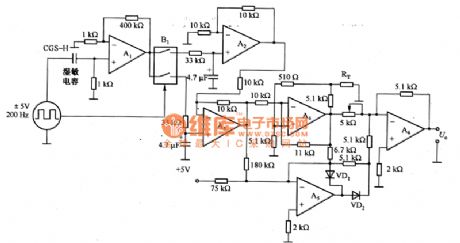
Picture 1 shows a circuit that uses the feature of low humidity of CGSH humicap to test other circuit. This circuit can even test other circuits with high accuracy under the atmosphere with less than 10% humidity. Operation amplifier A1, A2 and A3 are front amplifying circuit and difference amplifying circuit. The output signals of A1 pass through analog switch B1 and be alternately sent to A2 and A3 in order to eliminate the influence of change of temperature and the frequency noise and test steadily the output signals of sensor. A4,A5 and A6 are linear regulating circuit of sensor CGS-H and compensate the temperature by using the thermistor RL. (View)
View full Circuit Diagram | Comments | Reading(722)
TMS3450NL Digital Clock Integrated Circuit Diagram
Published:2011/7/3 1:35:00 Author:Vicky | Keyword: Digital Clock Integrated Circuit
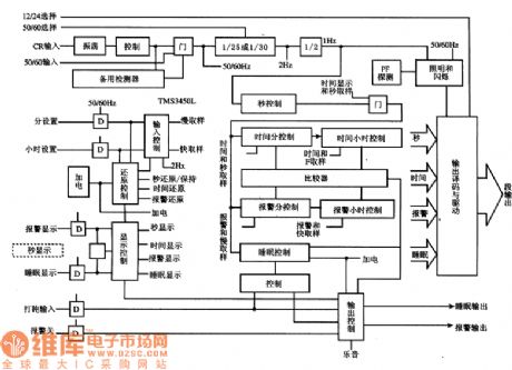
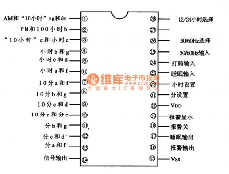
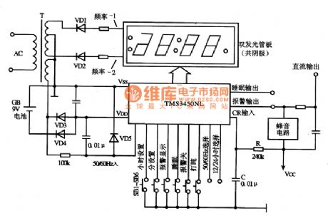
TMS3450NLis digital clock integrated circuit produced by Toshiba Corporation. It is widely used in various kinds of digital clock and auto clock circuit.
1 internal block circuit diagram and pin funtion
Internal block circuit diagram of TMS3450NL integrated circuit and the pin function are all shown in the above picture.
Internal block circuit diagram of IC TMS345ONL
Typical applied circuit of IC TMS345ONL
(View)
View full Circuit Diagram | Comments | Reading(20018)
AC power detecting circuit made by MD7750
Published:2011/6/21 8:10:00 Author:leo | Keyword: AC power detecting circuit made by MD7750, AD7750
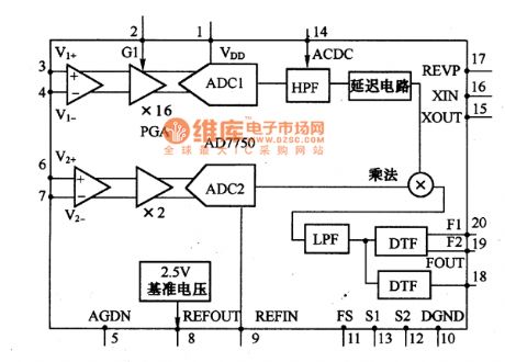
As picture a and b show, this is a AC power detecting circuit made by MD7750.AC power is the product of multiplication of current value and voltage value. This circuit is used to detect the power of 50 Hz single phase AC circuit. It can adopt common A/D converter but here it takes special A/D converter AD7750 with power detecting function.
The voltage value and current value can be tested on the high voltage terminal, therefore, current and voltage signals can be detected by voltage divider.AD7750 has two input terminals which are current signals terminal V1 and voltage signals terminal V2. These two terminals are different from each other. (View)
View full Circuit Diagram | Comments | Reading(744)
Power Factor Measure Circuit
Published:2011/5/20 18:49:00 Author:leo | Keyword: Power Factor Measure Circuit, CD4066
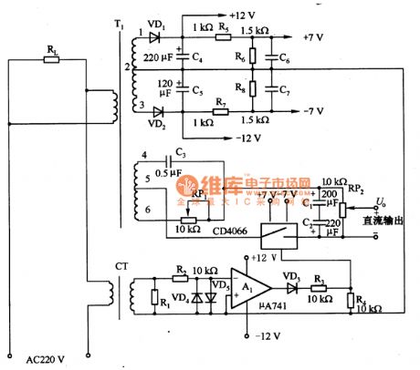
The picture is a power factor measure circuit. Power factor is used to show the phase relationship between voltage and electronic current. In the circuit, the voltage of T1 secondary 4 to 6 is used as the DC voltage sample and the secondary current of current transformer is used as the current sample. The current sample signal is amplified through A1 to control the analog switch CD4066 and takes effect with voltage sample, and then positive and negative DC voltages are generated.
(View)
View full Circuit Diagram | Comments | Reading(3677)
DC meter protection amplification circuit made by LM10 and others
Published:2011/5/20 18:52:00 Author:leo | Keyword: C meter protection amplification circuit, LM10
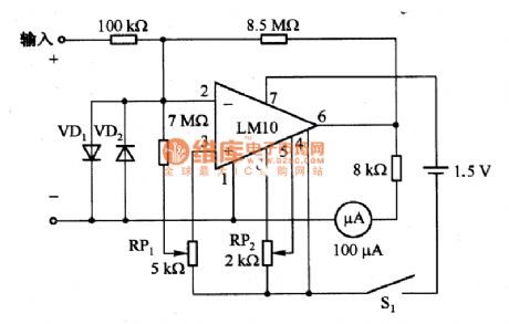
The picture 1 is a DC meter protection amplification circuit and is made up of LM10 and others. It is a kind of DC meter protection amplification circuit which needs to work in the temperature of 15 to 55 centigrade. The sensitivity of full scale is lOmV/l0nA. RP2 is used to set to zero. And the based voltage of setting zero is decided by the based voltage in the LM10 and does not affect by the voltage of power supply. RP1 is used to set bias current and VD1 and VD2 are the protecting diodes of LM10. The power supply of this circuit is 1.5 V and the current sinking is about 0.5mA.
(View)
View full Circuit Diagram | Comments | Reading(1042)
Projectile Speed Test Circuit Diagram
Published:2011/5/20 20:57:00 Author:leo | Keyword: Projectile Speed Test Circuit Diagram, HCT4060, 4096, MOSFET
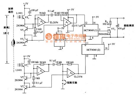
The picture shows a projectile speed test circuit. In the circuit, VT1 and VT2 are phototransistors. Projectile speed begins to be tested when the projectile passes through VT1. When projectile shades VT1, it can be considered as adding 500μV pulse to non-inverting input of A1. The pulse is amplified and reversed through A1 and A4 and offer starting impulse for HCT4060(2)-the 14 bits asynchronous counter. After this, the path of projectile is calculated again from zero and the speed will be calculated by 250ns resolution. At the same time, when projectile reaches VT2, it begins to test HCT4060(1) to test the destination of the projectile. (View)
View full Circuit Diagram | Comments | Reading(1375)
The high-end current monitor circuit formed by AD202
Published:2011/6/8 21:07:00 Author:leo | Keyword: The high-end current monitor circuit formed by AD202, AD202
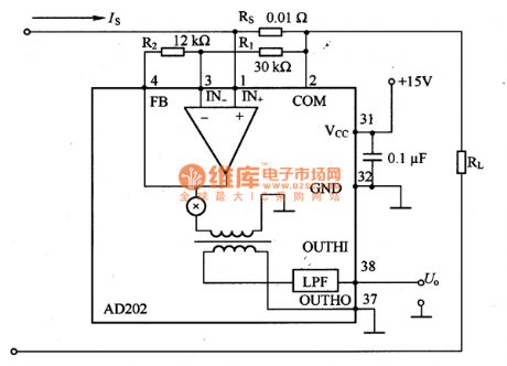
What the picture shows is a high-end current monitor circuit formed by AD202 and others. AD202 is a kind of amplifier that has inner transformer isolation. In this circuit, the maximum valve of power supply voltage is decided by voltage resistance of AD202. The voltage resistance of AD202 is 750 V which can meet the practical application needs. (View)
View full Circuit Diagram | Comments | Reading(1058)
The high-end current monitor circuit formed by OP184
Published:2011/6/8 21:12:00 Author:leo | Keyword: The high-end current monitor circuit formed by OP184, 2SA970, OP184, MOSFET
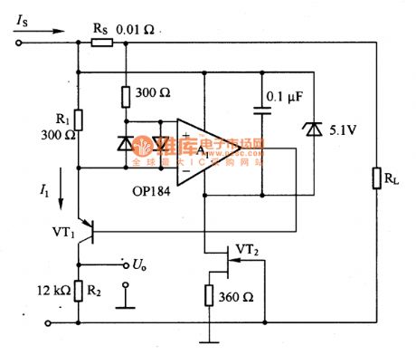
The picture shows a high-end current monitor circuit formed by OP184. In this circuit, A1 adopts OP184 operating amplifier. VT1 adopts 2SA970 transistor. When Is comes close to OA, the collector cutoff current of VT1 is the main factor that causes differences. When VT1 selects P channel JFET, it can improve detection precision. Now JFET with high pressure resistance is rare. So P channel MOSFET can be used instead of it. Using high degree accuracy resistance will also improve the detecting accuracy. (View)
View full Circuit Diagram | Comments | Reading(1778)
The circuit diagram of amplier formed by 2SJ114
Published:2011/6/8 21:34:00 Author:leo | Keyword: The circuit diagram of amplier formed by 2SJ114, 2SJ114
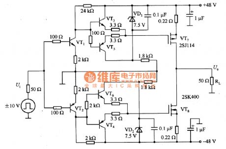
The picture 1 shows a amplifier circuit formed by 2SJ114.It can amplify square wave signal of ±l0V to ±48V. This circuit adopts P channel and N channel power MOSFET(VT7 and VT8) to form switch circuit. And the switch circuit is symmetry in the face and the below sides, so it can output dual polarity voltage. Due to the operating mode of VT7 and VT8 (the same power source), it needs to use VT3 to VT6 transistors to form the low resistance drive circuit in order to improve the response speed of gates. (View)
View full Circuit Diagram | Comments | Reading(3499)
The high-end current monitor circuit formed by INA168
Published:2011/6/8 21:50:00 Author:leo | Keyword: The high-end current monitor circuit formed by INA168, INA168
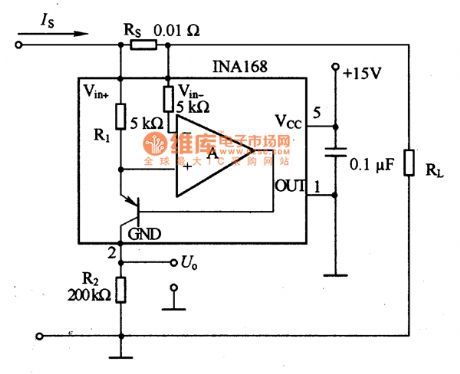
What the picture shows is a high-end current monitor circuit formed by INA168. When detecting the changing current of the power supply, loop wire is connected to the ground by the side. Sometimes, the enclosure and rock can not be connected to diverge resistance, it needs to connect Rs to the plus terminal of power supply to test the voltage difference generating by the current passing through Rs in order to detect the current passed through.
In this circuit, INA168 is specailly used to detect the current. The followings are some parameters of it: The voltage of power supply is 30 to 60 V. The maximum current it can detect is 10 A. When the current value is 10 A, the output detecting voltage should be 4 V. When the detecting voltage of power supply is low, it needs to use operating amplifier to form differential amplifier. But this circuit is suitable for the application under high power supply. (View)
View full Circuit Diagram | Comments | Reading(1977)
The low-end current monitor circuit formed by AD8551
Published:2011/6/9 2:47:00 Author:leo | Keyword: The low-end current monitor circuit formed by AD8551, AD8551

The picture shows a low-end current monitor circuit formed by AD8551, which is used to detect the motor current or charging current. When detecting the current of the motor or rechargeable battery, high-end monitor is frequently used, which is usually used to detect the power sourcing current.
In this circuit, A1 adopts highly accurate operating amplifier AD8551 which uses +2.7 to +5V signal power source to operate. (View)
View full Circuit Diagram | Comments | Reading(1921)
Overvoltage Detection Circuit Diagram formed by LTC1541 and Others
Published:2011/5/21 21:34:00 Author:leo | Keyword: Overvoltage Detection Circuit Diagram formed by LTC1541 and Others, 1N4005, ZTX458, 100K, 300K, 600V, LTC1541, 240V
As the picture shows, this is a overvoltage detection circuit. It is applied to detect the overvoltage in any power supply circuit with a detection scale from 3 V to hundreds of voltage. Besides, it can also be used to lock detect the voltage which can detect 30μs transient overvoltage peak pulse. Under the common condition, the current consumption of this circuit will be under 25μA. So it is the best voltage control circuit in the battery power supply system.
LTC1541 applied in this circuit is a kind of integrated circuit which contains a comparator A1 that has a small power compensation, operating amplifier A2 as well as UREF with the referred voltage of 1.20 V. This circuit demands a maximum of 13μA. (View)
View full Circuit Diagram | Comments | Reading(682)
Digital Meter Panel Circuit Diagram made up of PIC16C711 and Others
Published:2011/5/20 22:13:00 Author:leo | Keyword: Digital Meter Panel Circuit Diagram made up of PIC16C711 and Others, PIC16C711
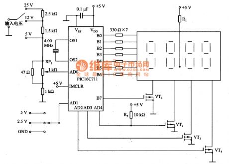
As the picture shows, this is a electrical digital meter panel circuit. As a 8 bits A/D converter, PIC16C711 has two input ports. Among them, AD0 is voltage input port and AD1 is scale selecting input port. If AD1 is connected to ground, it will show a scale of 0.00 V to 5.10 V with resolution of 20 mV. If AD1 is connected to 2.5V voltage, it will show a scale of 00.00 V to 12.75 V with the resolution of 50 mV. If AD1 is connected to 5 V, it will show a scale of 00.0 V to 25. 5 V and the resolution will be 100 mV. Under the common condition, PIC16C711 display accuracy is ±1/2LSB. It can drive four seven-port LED at the same time and only one LED can be lighted at one time. The input voltages of PIC16C711 are 5 V, 12 V and 25 V. (View)
View full Circuit Diagram | Comments | Reading(5211)
Voltage Amplifier Circuit Made up of LF356 and Others
Published:2011/5/20 19:55:00 Author:leo | Keyword: Voltage Amplifier Circuit Made up of LF356 and Others, LF356
What the picture 1 shows is a voltage amplifier circuit which is made up of LF356 and others. The voltage gain of this circuit is decided by the ratio of R1 and R2( R3 and R4).It can be calculated through the parameters that are shown in the picture that voltage gain is about 20 dB. R1 and R2 can make up of a degenerative circuit which is also be called small local hysteresis loss circuit that can prevent the circuit from close or uncommon oscillation. VD1 and VD2 are protection circuits of input port. (View)
View full Circuit Diagram | Comments | Reading(3740)
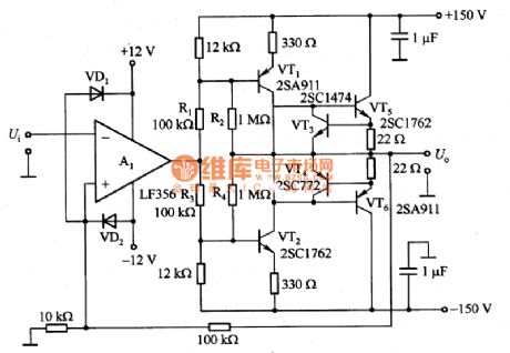
High Performance Complex Amplifier Circuit
Published:2011/3/29 21:58:00 Author:may | Keyword: High Performance, Complex Amplifier
High Performance Complex Amplifier Circuit is as follows:
(View)
View full Circuit Diagram | Comments | Reading(778)
| Pages:1/2 12 |
Circuit Categories
power supply circuit
Amplifier Circuit
Basic Circuit
LED and Light Circuit
Sensor Circuit
Signal Processing
Electrical Equipment Circuit
Control Circuit
Remote Control Circuit
A/D-D/A Converter Circuit
Audio Circuit
Measuring and Test Circuit
Communication Circuit
Computer-Related Circuit
555 Circuit
Automotive Circuit
Repairing Circuit