
Amplifier Circuits-RF
Index 2
The power amplifying circuit formed by LM377 and others
Published:2011/6/1 22:41:00 Author:leo | Keyword: The power amplifying circuit formed by LM377 and others, LM377
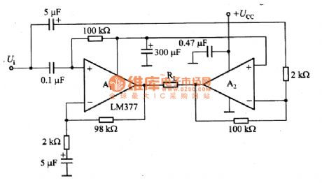
Picture 1 is a power amplifying circuit formed by LM377 and others. LC377 is a integrated circuit which has two in-die power amplifiers. If making the two power amplifiers connecting as electronic bridge, it can supply double power in valve to floating land negative load RL. Negative load RL can be servo motor or speaker. A1 and DC output port has the same electric potential, so it can not be connected to the stop capacitor with large capability.
When the negative load is 8 to 16 Ω, the response frequency of the circuit is 20Hz-160 KHz. When output power is 4W, the distortion of middle frequency is 0.1%. And when output power is 50mW, the distortion of middle frequency is 0.5%. (View)
View full Circuit Diagram | Comments | Reading(1445)
The high input resistance amplifier circuit formed by FET
Published:2011/6/8 22:13:00 Author:leo | Keyword: The high input resistance amplifier circuit formed by FET
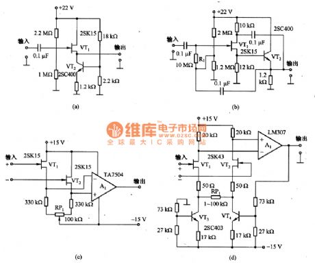
The picture 1 shows a high input resistance amplifier circuit. The picture 1(a) is the sourcing follower circuit formed by FET. The voltage gain of the follower: Av=gmRL/(l+gmRL); gm is mutual conductance; RL is sourcing load resistance. If Ac needs to be near 1, FET with bigger gm value is needed with the resistance value RL as big as possible. In order to increase the RL value, constant sourcing current formed by VT2 is adopted.
The picture1 (b) is the high input resistance circuit formed by FET. R1 is the grid offset deciding resistance. The current pass through R1 is usually very small. So the resistance is super high in the circuit.The Picture1 (c) is the circuit connected to operational amplifier. It is made up of two simple FET. RP1 is used to investigate the offset voltage. (View)
View full Circuit Diagram | Comments | Reading(1697)
The circuit diagram of preamplifier made by MC1709 serves the electric motor drive
Published:2011/6/1 22:33:00 Author:leo | Keyword: The circuit diagram of preamplifier made by MC1709 serves the electric motor drive, MC1709
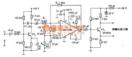
What Picture 1 shows is a kind of preamplifier made by MC1709 serves the electric motor drive circuit. In this circuit, the voltage plus of symbolic amplifier circuit is 39 dB. The circuit is made up of MC1709 and so on. The bandwidth of amplifier is 41 KHz which is decided by R5 and C2.Its single-ended output passes through the phase position of VT2 and is divided into two signals with discrepancy of 180 degree angle. This process will drive sh-pull (PP) output amplifier.
(View)
View full Circuit Diagram | Comments | Reading(1988)
The circuit diagram of preamplifier made by MC1437 serves the electric motor drive
Published:2011/6/1 22:36:00 Author:leo | Keyword: The circuit diagram of preamplifier made by MC1437 serves the electric motor drive, MC1437
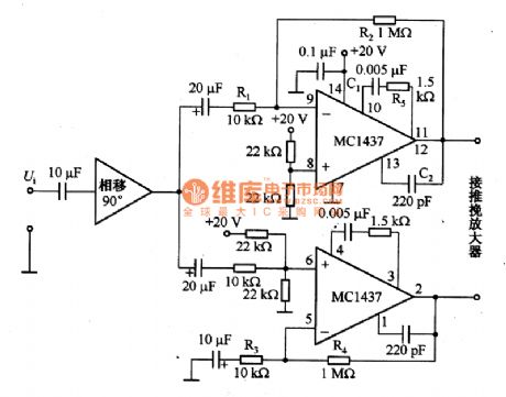
What Picture 1 shows is a kind of preamplifier made by MC1437 serves the electric motor drive circuit. In this circuit, the voltage plus of symbolic amplifier circuit is 39 dB. The circuit is made up of MC1709 and so on. The bandwidth of amplifier is 41KHz which is decided by R5 and C2.Its single-ended output passes through the phase position of VT2 and is divided into two signals with discrepancy of 180 degree angle. This process will drive sh-pull (PP) output amplifier. (View)
View full Circuit Diagram | Comments | Reading(987)
869~894MHz Narrow-Band Amplification Circuit Composed Of RF2320/2360
Published:2011/5/5 0:58:00 Author:Robert | Keyword: 869~894MHz, Narrow-Band, Amplification
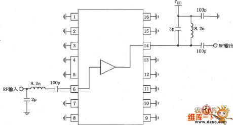
The picture shows the 869~894MHz narrow-band amplification circuit composed of RF2320/2360. The RF signal inputs from the 6 foot and outputed from the 14 foot through the amplifier. The 6 foot is coupling with internal amplifier, so it needs to add a 100pF blocking coupling capacitor (make up input matching networks with 8.2nH inductor). The 14 foot is output port and can be added to power Vdd through matching inductor. If users only consider aboutthe drift current, it only needs to add one choke coil.
(View)
View full Circuit Diagram | Comments | Reading(572)
RF2360 Linear General Purpose Amplifier Pin Circuit
Published:2011/5/5 0:58:00 Author:Robert | Keyword: Linear, General Purpose Amplifier, Pin
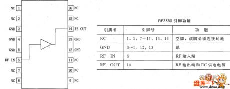
The RF2360 is a general purpose, low-cost, high-linearity RF amplifier IC, and is manufactured on an advanced gallium arsenideheterojunction bipolar transistor (HBT) process. It has been designed for using as an easily cascadable 75Ω gain block with a noise figure of less than 2dB. Gain flatness is better than 0.5dB from 5MHz to 1000MHz, and high linearity makes this part ideal for cable TV applications. Other applications are include IF and RF amplification in wireless voice and data communication products which operating in frequency bands up to 1000MHz. The device is self-contained with 75Ω input and output impedances providing less than 2:1 VSWR matching. RF2360 is featured in a SOP-16 squaredbatwing package, and its pinout is shown in the picture below.
(View)
View full Circuit Diagram | Comments | Reading(709)
880MHz Low Noise Amplification Application Circuit Composed Of RF2347
Published:2011/5/3 20:00:00 Author:Robert | Keyword: 880MHz, Low Noise, Amplification, Application
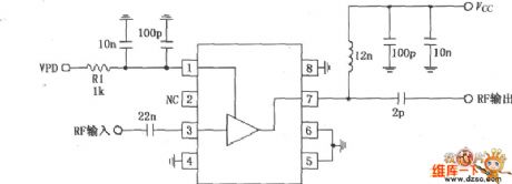
This pictureshown below is the 880MHz low noise amplification application circuit composed of RF2347. The RF signal is inputed to the 3 foot, and is outputed from 7 foot after amplification in the amplifiers. The 3 footis directly coupled with the internal amplifier, so a 22pF block-DC coupling capacitor is added outside the 3 foot, and therelated resistance would be 50Ω when working at 836MHz. The 7 foot is the output port of the open collector electrode, which can be connected to power Vcc through choke coil or matching inductor. This foot's typical matching resistance is 50Ω, and can be connected to external output-matching networks to suit the amplifier's output resistance, so that can get the maximum output power and efficiency. The 1 foot is for power down control terminal, which is used to control the drift current. When VPD=(2.8±0.1)V (Typical IPD is 8.5mA) the circuit begins to work; when VPD<0.9V the circuit becomes closed; VPD reqiures external RF bypass circuit.
(View)
View full Circuit Diagram | Comments | Reading(582)
Principle Circuit of Mixer with 6 Input Channels
Published:2011/5/3 2:30:00 Author:Felicity | Keyword: Principle Circuit of Mixer with 6 Input Channels,
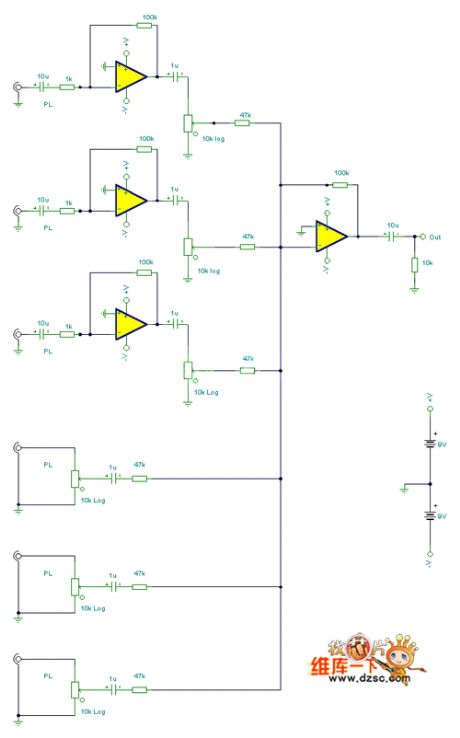
Principle Circuit of Mixer with 6 Input Channels is showed in the picture above. (View)
View full Circuit Diagram | Comments | Reading(622)
915MHz RF amplifier circuit composed of RF2103P
Published:2011/4/11 2:36:00 Author:may | Keyword: RF amplifier
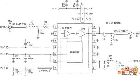
The picture is 915MHz RF amplifier circuit composed of RF2103P. P1 is socket, among which, P1-1 connect power Vcc, P1-2 connect ground, P1-3 connect power down control voltage VB; J2 is RF output socket.
(View)
View full Circuit Diagram | Comments | Reading(987)
75Ω Impedance Linear Amplification Circuit Consists Of RF2320
Published:2011/4/24 6:02:00 Author:Robert | Keyword: 75Ω, Impedance Linear Amplification

75Ω Impedance Linear Amplification Circuit Consists Of RF2320 is shown below. J1 and J2are 75Ω Connectors.
(View)
View full Circuit Diagram | Comments | Reading(592)
4W power amplifier circuit of integrated amplifier
Published:2011/3/29 21:56:00 Author:may | Keyword: Integrated Amplifier, 4W, Power Amplifier

4W power amplifier circuit of integrated amplifier is shown in the diagram:
(View)
View full Circuit Diagram | Comments | Reading(1211)
| Pages:2/2 12 |
Circuit Categories
power supply circuit
Amplifier Circuit
Basic Circuit
LED and Light Circuit
Sensor Circuit
Signal Processing
Electrical Equipment Circuit
Control Circuit
Remote Control Circuit
A/D-D/A Converter Circuit
Audio Circuit
Measuring and Test Circuit
Communication Circuit
Computer-Related Circuit
555 Circuit
Automotive Circuit
Repairing Circuit