
Amplifier Circuits-RF
Index
RF amplifier principle circuit composed of RF2103P
Published:2011/10/26 21:11:00 Author:May | Keyword: RF amplifier
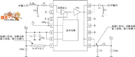
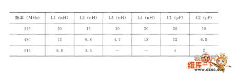
RF signal (RF) isinput by pin 1, enlarged by preamplifier and final power amplifier ( FPA), thenoutput by pin 14. There is a blocking coupling capacitor between pin 1 and preamplifier, so it does not need to add coupling capacitor. Output ends pin 8, 9, 13, 14 are connected inside of the chip. Normally, pin 13, 14 are connected outside to be uses the as signal output, which connects to the matching network to make the amplifier output resistance match with it, then it gets themaximum output power and efficiency; and pin 8, 9 are connectedoutsideto beas power supply end, when it works at 915MHz, it adds a filter capacitor C2(=2pF) to ground tomake up filter circuitwith second harmonic, which can shortconnect second harmonic effectively.
(View)
View full Circuit Diagram | Comments | Reading(1321)
Small FM transmitter ( wireless speaker) circuit
Published:2011/10/31 3:02:00 Author:May | Keyword: FM transmitter, wireless speaker
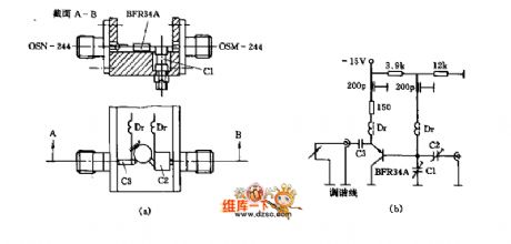
This circuit consists of transistor BFR34A,and the figure(a) shows its mechanical structure, when it worksat operating point, Uce=12V, Ic=17mA, theoutput power is12mW.Figure (b) is thebasic circuit. The collector's pins are grounded for better heatdissipation. The optimal phase condition of feedback between tmitter and collector isadjustedby coaxial wire. Variable output coupling capacitor is composed of the small thin plate with side length in5mm.
(View)
View full Circuit Diagram | Comments | Reading(2104)
RF_PREAMPLIFIERS
Published:2009/6/18 2:27:00 Author:May
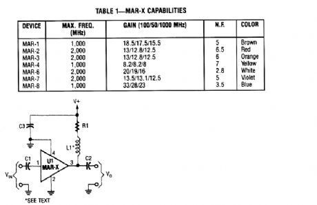
In this basic MAR-x-based circuit, both the input and output are comprised of a single dc-blocking capacitor (C1 and C2 for the input and output, respectively). The dc power-supply net-work (comprised of L1 and BI) is attached to the MAR-x via the RF-output terminal (lead 3). (View)
View full Circuit Diagram | Comments | Reading(992)
5_W_7_MHz_RF_POWER_AMPLIFIER
Published:2009/6/18 2:16:00 Author:May
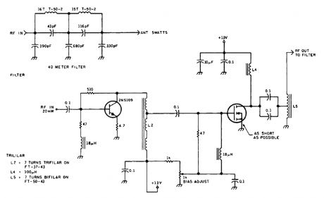
The circuit shown will produce up to 5-W RE output in the 40-m (7 MHz) amateur band. The coils shown are wound on toroidal cores (Armdon Associates Inc.). The part numbers are given in the schematic. The circuit requires about 20-mW drive and a 13-V supply. (View)
View full Circuit Diagram | Comments | Reading(787)
SWITCHABLE_HF_VHF_ACTIVE_ANTENNA
Published:2009/6/18 2:10:00 Author:May
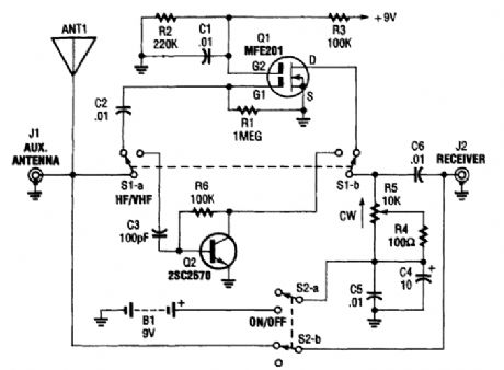
The AA-7 active antenna contains only two active elements: Q1 (an MFE201 N-channel dual-gate FET) and Q2 (a 2SC2570 npn VHF silicon transistor), which provide the basis of two indepen-dent, switchable RE preamplifiers. (View)
View full Circuit Diagram | Comments | Reading(2954)
70_MHz_RF_POWER_AMPLIFIER
Published:2009/6/17 23:38:00 Author:May
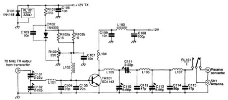
The SD1143 transistor provides a gain of about 14 dB in this circuit. It uses the fact that a 175-MHz device has a much higher gain when used at lower frequencies. The amplifier was originally de-signed to be used with a transverter. The output is 8 to 10 W for a 300- to 500-mW input. (View)
View full Circuit Diagram | Comments | Reading(1401)
BROADCAST_BAND_RF_AMPLIFIER
Published:2009/6/17 23:36:00 Author:May
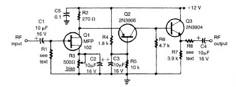
The circuit has a frequency response that ranges from lO0 Hz to 3 MHz; the gain is about 30 dB. Field-effect transistor Q1 is configured in the common-source self-biased mode; optional resistor R1 allows you to set the input impedance to any desired value. Commonly, it will be 50 Ω. The signal is then direct-coupled to Q2, a common-base circuit that isolates the input and output stages and pro-vides the amplifier's exceptional stability. Last, Q3 functions as an emitter-follower, to provide low output impedance (about 50 Ω). If you need higher output impedance, include resistor R8. It will af-fect impedance according to this formula:R8≈ROUT - 50. Otherwise, connect output capacitor C4 directly to the emitter of Q3. (View)
View full Circuit Diagram | Comments | Reading(0)
BROADBAND_RF_AMPLIFIER
Published:2009/6/17 23:19:00 Author:May
The use of a FET gives this amplifier a high input impedance. The bandwidth should be ade-quate for LW through HF use (dc-30 MHz), as an active antenna preamplifier. (View)
View full Circuit Diagram | Comments | Reading(3920)
Low-noise RF - IF amplifier circuit diagram
Published:2011/7/25 22:08:00 Author:Ecco | Keyword: Low-noise RF amplifier, IF amplifier
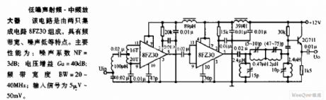
The circuit is composed of two 8FZ30 integrated circuits with wide frequency bandwidth, low noise. The main properties: voltage gain Gu = 40dB; bandwidth BW = 20 to 40MHz; input signal is 5μV to 50mV.
(View)
View full Circuit Diagram | Comments | Reading(1378)
TRF5O01 GPS RF receiving and collecting integrated circuit
Published:2011/7/13 20:07:00 Author:leo | Keyword: GPS, RF, Integrated circuit
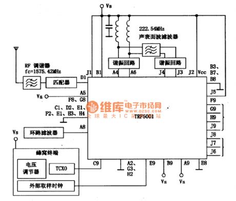
TRF5O01 is a type of GPS RF receiving and collecting integrated circuit used in GPS positioning system.
Function features:
TRF5O01 has the cellular terminal and emitter with sources. It contains low noise amplifier mixer. The first and second LO set-frequency synthesizer and four bit ADC and so on are always used in high sensibility GPS system. TRF5O01 working voltage is 2.7 V to 3.3 Vand the current consumption is super light. When the voltage is 2.7 V, its current consumption is 49 mA. (View)
View full Circuit Diagram | Comments | Reading(988)
The circuit diagram of a power MOSFET amplifier circuit with high frequency feature
Published:2011/7/13 19:49:00 Author:leo | Keyword: Power MOSFET amplifier, high frequency
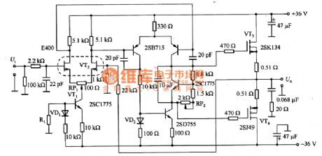
The picture 1 is a power MOSFET amplifier circuit with high frequency feature. In order to restrain the influence of the changes of power supply, it takes VT1 and VT2 to form the constant current circuit,while, VT3 and VT4 are end power amplifying circuit. Due to the influence of offset current, its drain currenthastemperature factors which is from positive to negative. Therefore, it uses RP2 to control the offset in order to set the drain current to 0.1 to 0.2 A, which passes through VT3 and VT4. And when its frequency is 1Hz to 800 kHz, the distortion is 0.04% per 1 kHz. At the same time, its output power is 40 W and the convert rate is 100V/μs. (View)
View full Circuit Diagram | Comments | Reading(2758)
FET bandwidth amplifier circuit
Published:2011/7/10 2:27:00 Author:leo | Keyword: FET, Bandwidth, Amplifier circuit

Picture 1 shows a FET bandwidth amplifier circuit. In this circuit, VT1 and VT2 are bumpers. VT1 is used as source follower, while VT3 and VT4 are used to amplifying voltage and VT5 and VT6 have the function of power amplifying. A1 is DC feedback circuit which is used to stabilize the circuit. And A1 compares the output signals and input signals and amplifies the difference of them. The amplified signals offer differential to VT2, as a result, VT1 channel current is permitted to form a circle. And this demands that the UGS of VT1 should be matched with input and output voltage of the circuit. (View)
View full Circuit Diagram | Comments | Reading(1141)
New smart phone manager circuit
Published:2011/7/8 1:13:00 Author:Fiona | Keyword: New smart phone, manager
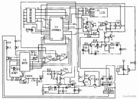
New smart phone manager circuit is shown as above,this device uses specific intelligent communications integrated controller chip ZH988A for the communications for the core to compose the smart phone manger, the circuit is shown as below. Its main functions are: 1 every phone can beset up19 users, the user has independent password and account, it achieves household management;2 limit each of user to do permissions, costs plan and so on; 3 open 110,119,114 and other free items; 4 automatically calculate the holding time and cost; 5 the data and passwords can be modified by keyboard;6 securitybeat monitoring;7 P / T is compatible and so on.
(View)
View full Circuit Diagram | Comments | Reading(1814)
IF amplifier IC circuit
Published:2011/6/19 4:47:00 Author:John | Keyword: IF amplifier
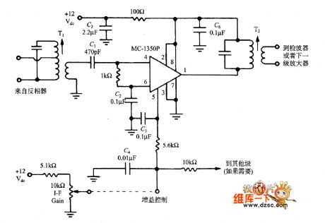
The picture shows a basic circuit composed of IF amplifier module. If a local reception of AM receiver is needed, the first-level circuit is only needed. For receivers with short-wave or other needed high-sensitivity, two or three circuits are needed to increase the gain. Each level of the gain requires 50dB and some projects may require 80 ~ 110dB.
IF amplifier module is constructed based MC-1350P gain module chip (the chip can also replace NTE-746 in the NTE). (View)
View full Circuit Diagram | Comments | Reading(2048)
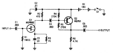
Simple transistor IF amplifier circuit
Published:2011/6/17 9:49:00 Author:John | Keyword: transistor, IF amplifier
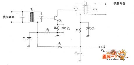
A simple IF amplifier is just as shown in the figure. AM band radio may have such a circuit, but FM receiver, shortwave receivers and other types of communications receivers may have two to four such circuits.
figure: Simple transistor IF amplifier circuit (View)
View full Circuit Diagram | Comments | Reading(3568)
SL56OC IF amplifier circuit
Published:2011/6/17 10:51:00 Author:John | Keyword: IF amplifier
A tuning circuit is as shown in the following. Tuned circuit T1 is used to replace the original input circuit. Output circuit is replaced with the transformer T2. Besides, V + terminal circuit here uses a Zener diode to rectifier the DC voltage.
figure: SL56OC IF amplifier circuit (View)
View full Circuit Diagram | Comments | Reading(803)
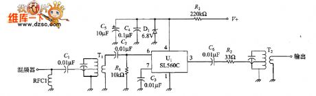
SL-560C IF amplifier circuit
Published:2011/6/17 10:46:00 Author:John | Keyword: IF amplifier
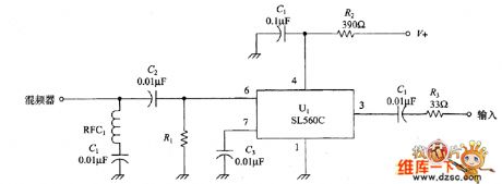
SL560C is basically a gain block that can be used in RF and IF frequency area. Figure shows a circuit based on SL560C. SL560C is the single-ended output circuit transferred by differential input. And the used input end needs to be set by the bypass of capacitor C3. Since this is a broadband circuit, the input or output circuit has no tuning function. The input circuit includes a 0.02μF input coupling capacitor and an RF choke (RFC1).
figure: SL-560C IF amplifier circuit (View)
View full Circuit Diagram | Comments | Reading(1502)
The circuit diagram of amplifier made up of μA709
Published:2011/6/8 20:53:00 Author:leo | Keyword: The circuit diagram of amplifier made up of μA709 , A709
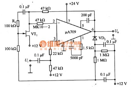
Picture 1 shows an amplifier made up ofμA709 and others. In this circuit, VT1 forms step attenuator which is regarded as a control part of automatically gaining. It is used to rectify and feedback the peak valve of its gate bias and connected to the negative feedback circuit of operating amplifierμA709.Feeback generated through R1 is used to make up nonlinear distortion of VT1. (View)
View full Circuit Diagram | Comments | Reading(854)
The circuit diagram of preamplifier serving the electric motor drive circuit
Published:2011/6/1 22:31:00 Author:leo | Keyword: The circuit diagram of preamplifier serving the electric motor drive circuit, MC1437
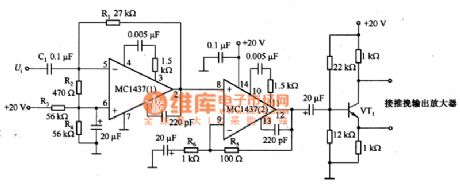
Picture 1 shows a preamplifier that serves the electric motor drive circuit. In this circuit, 90° phase shift adopts differential coefficient circuit with operational amplifier MC1437 (1). It is connected to in-phase amplifier MC1437 (2) with the voltage plus of 40 dB. Feedback resistance R1 and input capacitance C1 can make up of differential circuit. R3 and R4 are used to set DC operating point of operational amplifier. And the operating point is set in the 1/2 of the voltage of power supply. The gain of differential circuit increases by the frequency. Therefore, the circuit may develop into high-frequency section and it needs to limit bandwidth. The single-ended output of MC1437 (2) passes VT1 and becomes two ways signals in order to drive sh-pull (PP) output amplifier. (View)
View full Circuit Diagram | Comments | Reading(699)
The push-pull power amplifier circuit formed by MOSFET
Published:2011/6/9 3:02:00 Author:leo | Keyword: The push-pull power amplifier circuit formed by MOSFET
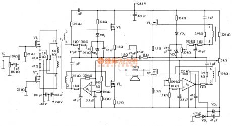
The picture 1 shows a push-pull power amplifier circuit formed by MOSFET. VT1 and VT2 form the propel circuit, which uses transformer T1 to get the same output value but different polarity signals. And the signals are driven separately by the power output ports formed by VT3 and VT4 (VT5 and VT6). In order to increase output power, when the operating power is 1 kHz, the minimum distortion is 0.25%. The voltage gain of median frequency period is 31.5 dB.When voltage gain is -3dB, the bandwidth is narrow, which is 11 kHz to 16.8 kHz. When input port is short or cut off, noise voltage is 0.22 mV. So it has excellent performance.
(View)
View full Circuit Diagram | Comments | Reading(2948)
| Pages:1/2 12 |
Circuit Categories
power supply circuit
Amplifier Circuit
Basic Circuit
LED and Light Circuit
Sensor Circuit
Signal Processing
Electrical Equipment Circuit
Control Circuit
Remote Control Circuit
A/D-D/A Converter Circuit
Audio Circuit
Measuring and Test Circuit
Communication Circuit
Computer-Related Circuit
555 Circuit
Automotive Circuit
Repairing Circuit