
Index 350
74 series digital circuit 74LS379 eight D flip flop
Published:2011/5/13 5:08:00 Author:May | Keyword: digital, eight, D flip flop
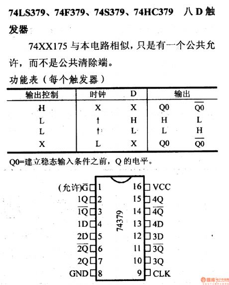
74LS379, 74F379, 74S379, 74HC379 eight D flip flop74××175 is similar to this circuit. It only has one common allow end, and not common clear end.function table ( every flip flop)Q0=the level of Q before building stable state input condition
(View)
View full Circuit Diagram | Comments | Reading(1518)
74 series digital circuit 74LS378 74F378 and other six D flip-flop
Published:2011/5/13 5:08:00 Author:May | Keyword: digital, six D flip-flop
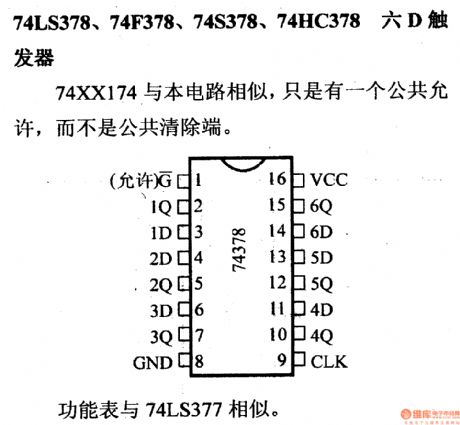
74LS378, 74F378, 74S378, 74HC378 six D trigger74××174 is similar to this circuit. It only has one public permitting but not public clearing end. (View)
View full Circuit Diagram | Comments | Reading(676)
74 series digital circuit 74LS377 and other eight D flip-flop
Published:2011/5/13 5:06:00 Author:May | Keyword: digital, eight D flip-flop
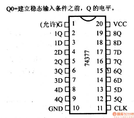
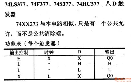
Q0=the level of Q before building stability input condition.74LS377, 74F377, 74S377, 74HC377 eight D trigger74××273 is similar to this circuit. It only has one public permitting but not public clearing end. (View)
View full Circuit Diagram | Comments | Reading(701)
FREQUENCY_DIVIDER_FOR_10_MHz_FREQUENCY_STANDARD
Published:2009/6/19 2:28:00 Author:May
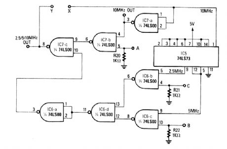
View full Circuit Diagram | Comments | Reading(697)
74 Series digital circuit 74376 four J-K non-flip-flop
Published:2011/5/13 5:02:00 Author:May | Keyword: digital, four J-K, non-flip-flop
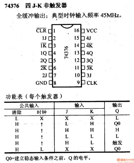
74376 four J-K non-triggerfull buffer output: typical clock input frequency is 45MHz
(View)
View full Circuit Diagram | Comments | Reading(664)
VSB_FILTER_FOR_LM2889
Published:2009/6/19 2:27:00 Author:May
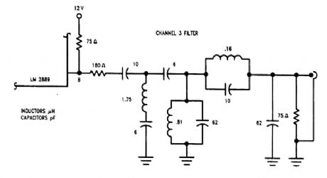
This filter is for CH3, in order to get a vestigial sideband TV signal. It is designed for 75-Ω im-pedance levels. (View)
View full Circuit Diagram | Comments | Reading(612)
74 Series digital circuit 74S340 74S341 and other eight buffer/line driver (three-state)
Published:2011/5/11 3:57:00 Author:May | Keyword: digital, eight buffer, line driver, three-state
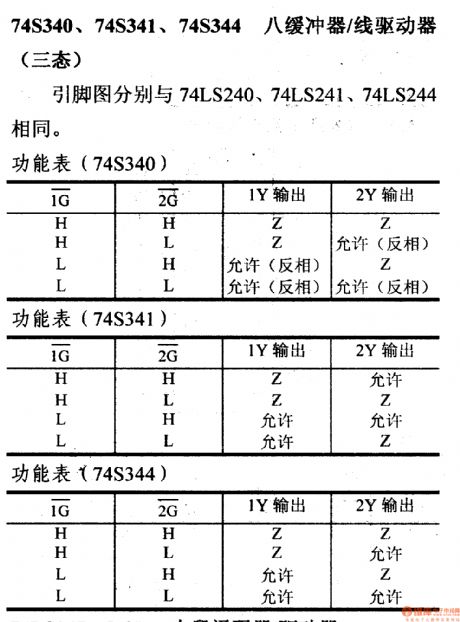
74S340, 74S341, 74S344 eight buffer/line driver (tristate)Their pin diagrams is seperately same as 74LS240, 74LS241, 74LS244.
(View)
View full Circuit Diagram | Comments | Reading(509)
VOLTAGE_CONTROLLED_LOW_PASS_FILTER
Published:2009/6/19 2:26:00 Author:May
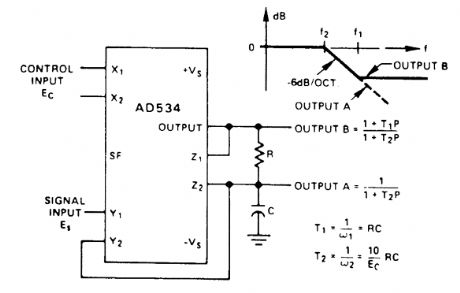
The voltage at Output A, which should be unloaded by a follower, responds as though ES were di-rected to the RC filter, but the filter's break frequency were proportional to Ec[i.e,.=Ec/(20πRC)] The frequency response has a break at f2; and the 6-dB/octave rolloff. The voltage at Output B has the same response, up to [f1 (f = 1/(20πRC)], then levels off at a constant attenuation of f2/f1 = Ec\10.For example, if R = 8kΩ, C = 0.002μF, Output A has a pole at 100 Hz to 10 kHz and can be loaded.The circuit can be converted to high-pass by interchanging C and R. (View)
View full Circuit Diagram | Comments | Reading(1)
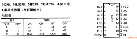
74 Series digital circuit 74298 74LS298 and other 4-bit 2 selects 1 data selector (register output)
Published:2011/5/11 3:58:00 Author:May | Keyword: digital, 4-bit, 2 selection 1, data selector, register output
View full Circuit Diagram | Comments | Reading(892)
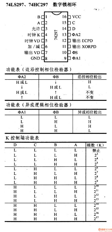
74 series digital circuit 74LS297 74HC297 and other digital phase-locked loop
Published:2011/5/11 3:59:00 Author:May | Keyword: digital, digital phase-locked loop
View full Circuit Diagram | Comments | Reading(865)
TYPICAL_TWO_WAY_SWITCH_WIRING
Published:2009/6/19 2:23:00 Author:May
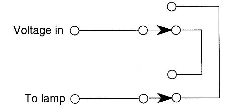
When the light is off, it can be turned on with either switch. When it's on, it can be turned off with either switch. (View)
View full Circuit Diagram | Comments | Reading(620)
74 series digital circuit 74166 74LS166 and other eight bits shift registers (serial/parallel-serial out)
Published:2011/5/11 3:59:00 Author:May | Keyword: digital, eight bits, shift register, serial/serial/parallel out
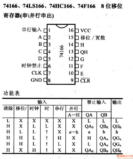
View full Circuit Diagram | Comments | Reading(2932)
CIGRETTE_LIGHTER_9_V_ADAPTER
Published:2009/6/19 2:18:00 Author:May
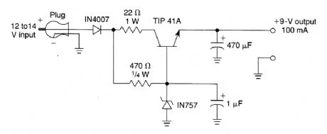
A simple way to provide +9 V at 100 mA from a 12-V auto source. Applications include small radios, cassettes, etc. (View)
View full Circuit Diagram | Comments | Reading(660)
DIGITAL_COMB_FILTER
Published:2009/6/19 2:18:00 Author:May
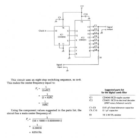
View full Circuit Diagram | Comments | Reading(781)
ADJUSTABLE_Q_NOTCH_FILTER
Published:2009/6/19 2:17:00 Author:May
This figure shows a circuit where the Q can be varied from 0.3 to 50. A fraction of the output is fed back to R3 and C3 by a second voltage follower, and the notch Q is dependent on the amount of signal fed back. A second follower is necessary to drive the twin T from a low-resistance source so that the notch frequency and depth will not change with the potentiometer setting. (View)
View full Circuit Diagram | Comments | Reading(0)
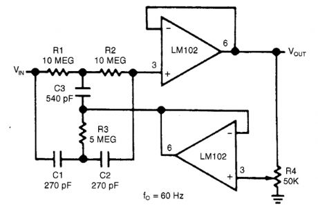
HIGH_Q_NOTCH_FILTER
Published:2009/6/19 2:16:00 Author:May
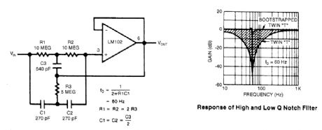
This shows a twin T network connected to an LM102 to form a high Q, 60-Hz notch filter. The Junction of R3 and C3: which is normally connected to ground, is bootstrapped to the output of the follower. Because the output of the follower is a very low impedance, neither the depth nor the frequency of the notch change; however, the Q is raised in proportion to the amount of signal fed back to R3 and C3. (View)
View full Circuit Diagram | Comments | Reading(0)
TRANSISTOR_MATCHING_CIRCUIT
Published:2009/6/19 2:11:00 Author:May
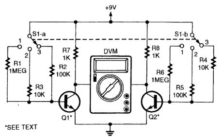
In order to match two transistors, select Q1 and Q2 so that they give zero readings(or as close as possible)on a DVM. The DVM acts as a null detector. An analog meter can be substituted. S1 should be set for an appropriate level of base current(approximately 8,80,or 800 μA). (View)
View full Circuit Diagram | Comments | Reading(1286)
REFERENCE_CIRCUIT
Published:2009/6/19 2:09:00 Author:May
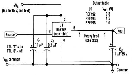
In this high-performance reference circuit, U1 is a device from the REF190 series producing de-vice-selectable outputs of 2.5, 4.5, and 5 V with simple, noncritical external circuitry. An Analog Devices REF 19 X(see the table in the figure)is used to derive a reference voltage. (View)
View full Circuit Diagram | Comments | Reading(799)
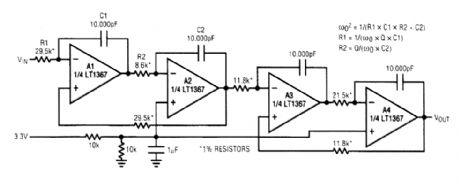
SINGLE_33_V_SUPPLY_4_POLE_STATE_VARIABLE_FILTER
Published:2009/6/19 2:09:00 Author:May
View full Circuit Diagram | Comments | Reading(510)
TWO_OP_AMP_BANDPASS_FILTER
Published:2009/6/19 2:08:00 Author:May


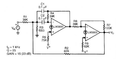
This circuit uses only two capacitors.The amplifier on the right supplies a controlled amount of characteristics. Resistors R5 and R8 are used to bias the outvoltage of the amplifiers at V+/2. (View)
View full Circuit Diagram | Comments | Reading(1)
| Pages:350/471 At 20341342343344345346347348349350351352353354355356357358359360Under 20 |
Circuit Categories
power supply circuit
Amplifier Circuit
Basic Circuit
LED and Light Circuit
Sensor Circuit
Signal Processing
Electrical Equipment Circuit
Control Circuit
Remote Control Circuit
A/D-D/A Converter Circuit
Audio Circuit
Measuring and Test Circuit
Communication Circuit
Computer-Related Circuit
555 Circuit
Automotive Circuit
Repairing Circuit