
Index 361
Battery Charging Circuit of LTC1541
Published:2011/7/19 11:11:00 Author:Michel | Keyword: Battery Charging Circuit
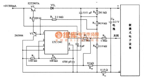
The above picture is battery charging circuit of LTC1541.It is charging circuit of portable electronic devices and LTC1541 is composed of reference voltage,comparator and operational amplifiers, etc. High precision reference voltage (plus or minus 0.4%) will adjust lithium-ion battery floating voltage to± 1.2% and this is the value that most manufacturers require.VT1 transistor is used to adjust battery charge current and operational amplifier input(feet 1) of LTC1541 amplifies VT1 base current via VT2.VD1 diode is to prevent reverse current circulation produced by adapter or power control failure.Because the circuit is linear regulators, VT1 power consumption needs to be considered. (View)
View full Circuit Diagram | Comments | Reading(529)
STR6465 Switch Power Thick Membrane Integrated Circuit
Published:2011/7/19 11:28:00 Author:Michel | Keyword: Switch Power , Thick Membrane, Integrated Circuit
TR6465 is switch power thick membrane integrated circuit of SANKEN and it is used in ChangHong CNl1 cassette mechanism color TVs such as H25K6O,G29E6,29K19,25K18 and PF28E18.
First,Functions and Features STR6465 integrated circuit contains error control circuit, start-up circuit, switch tube (field effect power switch tube), protection circuit, and some other auxiliary functions circuit
Second,Pins Functions and DataSTR6465 integrated circuit uses single inline package and its pins functions and data is shown as picture 1.
Table 1:Pins Functions and Data of STR6465 IC (View)
View full Circuit Diagram | Comments | Reading(533)
Ultralow Frequency Sawtooth Wave Generating Circuit
Published:2011/7/17 10:22:00 Author:Michel | Keyword: Ultralow Frequency, Sawtooth Wave, Generating Circuit
The above picture is a ultralow frequency sawtooth wave generating circuit.In order to perform the low frequency oscillation, positive and negative double power supply are provided.If VT1 pluses negative pulse signal, the VT1 stops, VT2 conducts, the power supply charges C1 via VT2.VT1 base potential rises as the charging current declines,VT1 conducts,VT2 stops at the same time.Meanwhile,C1 discharges via R1 and RP1 until VT2 conducts.Because R1 and RP1 determine VT2 conduction potential,the linear is output.0005 hz to dozens of KHZ oscillation frequency can be gotten when the C1 and (R1 + RRP1) value are changed. (View)
View full Circuit Diagram | Comments | Reading(497)
Pulse Width Modulation Circuit of NE555
Published:2011/7/17 10:22:00 Author:Michel | Keyword: Pulse Width, Modulation Circuit
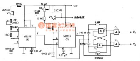
The above picture is pulse width modulation circuit composed of NE555.This circuit needs push-pull control pulse to generate switch power supply.NE555(1) is 40KFZ oscillator and its output triggers the trigger composed of NE555(2) monomultivibrator and gate circuits G1 and G2,which makes its oscillation frequency decline to 20kHZ and output two pulse signals via G3 and G4 push-pull.When control voltage is in lowest condition,NE555(1) oscillates on 40kHZ,NE555(2) pulse width is in widest situation.At this time,the dutyfactoris biggest,NE555(2) pulse becomes narrow as the control voltage increases.And if NE555(2) pulse width is in its narrowest condition,VT1 stops and NE555(1) oscillation frequency declines and the dutyfactor becomes less.If the control voltage is close to power source voltage, the NE555 (1) stop oscillatiing and the dutyfactor is zero. (View)
View full Circuit Diagram | Comments | Reading(2035)
DTMF Infrared Remote Controller of LM567 Encoder
Published:2011/7/17 10:24:00 Author:Michel | Keyword: Encoder, Infrared, Remote Controller
Besides special encoder, DTMF decode still can use phase locked loop audio decoder, LM567 to decode. But there is only one kind of frequency when the frequency signal is output after the
LM567 decoding.The frequencies output by two decoders constitute one group of control signals.As shown in the picture,infrared remote control signal is transmitted by DTMF and
infrared remote control switch is composed of two LM567 decoders.The circuit consists of twelve channel coding circuit DTMF infrared remote transmitters, infrared receiving voltage amplifier, the channel signal decoder, switch controller and relay and its driving circuit. (View)
View full Circuit Diagram | Comments | Reading(806)
Exportation Ringing Transmission and Leading Control Circuit
Published:2011/7/13 7:59:00 Author:Michel | Keyword: Ringing Transmission, Leading Control Circuit

Exportation Ringing Transmission and Leading Control Circuit
This picture is exportation ringing test signal transmission control and CD22100 writing enabling signalcontrol circuit.Its program is almost same with the control part of user circuit. (View)
View full Circuit Diagram | Comments | Reading(472)
Charging Circuit of MAX1879
Published:2011/7/19 11:04:00 Author:Michel | Keyword: Charging Circuit
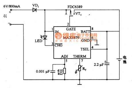
The above picture is charging circuit of MAX1879.When the power is switched on,precharging circuit conducts and LED blinks when the battery voltage is 2.2~2.5V.As the battery voltage is more than 2.5 V, the circuit turns into fast charging way and exchange adapter is used to limit battery charging current. As it is fast charging, LED blinks. If the battery voltage rises to 4.2 V, then it turns into pulse charging ways. The pulse minimum charging time is set by TSEL terminal. If the ratio of VT1 conduction time and the cut-off time are less than 1/8, it is judged as the longest time charging ways.6.25h timer starts and it keeps pulse charging ways and the timing time ends until the charging is over. (View)
View full Circuit Diagram | Comments | Reading(630)
SB6702 Communication Single Chip Microcomputer Integrated Circuit
Published:2011/7/19 11:30:00 Author:Michel | Keyword: Communication Single Chip, Microcomputer Integrated Circuit
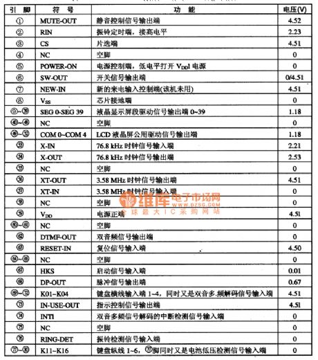
SB6702 is one SB6702 communication single-chip microcomputer integrated circuit which is widely used in caller identification telephones.
First,Functions and FeaturesSB6702 integrated circuit contains DTMF generator, low voltage detection circuit, liquid crystal display driver circuit,energy saving mode control circuit, the keyboard matrix switch circuit and caller id signal processing circuit.
Second,Pins Functions and DataSB6702 integrated circuit uses 80 feet encapsulation methods which is directly packaged on the four CMOS microprocessors of the printed circuit board and its pins functions and data are shown as table 1.
(View)
View full Circuit Diagram | Comments | Reading(472)
TDAl077 Microcomputer Dialing Integrated Circuit
Published:2011/7/19 11:29:00 Author:Michel | Keyword: Microcomputer, Dialing Integrated Circuit

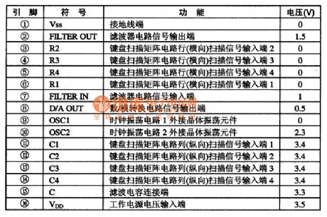
TDAl077 microcomputer dialing integrated circuit is often used in kinds of telephones.
One Functions and Features
TDA1077 integrated circuit contains key switch signal coder and dial signal processing circuit etc.
Two Pins Functions and Data
The pins function and data of TDA1077 integrated circuit are shown as table 3.
Table:Pins Functions and Data of TDA107 IC (View)
View full Circuit Diagram | Comments | Reading(562)
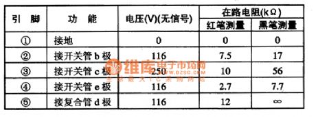
STR10006 Switch Power Thick Membrane Integrated Circuit
Published:2011/7/19 11:26:00 Author:Michel | Keyword: Switch Power, Thick Membrane, Integrated Circuit
STR10006 is switch power thick membrane integrated circuit of SANKEN and it is used for big TV screens, the deputy of switch power supply screens.
First,Functions and Features
STRlO006 integrated circuit contains RCC control system and power switch tube, sampling error signal processing circuit,other auxiliary power supply circuit and the protection circuit etc.
Second,Pins and Data
STR10006 integrated circuit uses pins single in-line package and its pins functions and dataare shown as table 1.The data is measured via the Panasonic TC-29GVl2G type big TV screen by using U2O1 type multimeter. (View)
View full Circuit Diagram | Comments | Reading(1206)
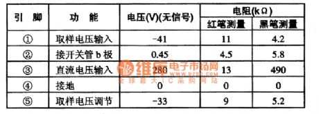
STR51213 Switch Power Thick Membrane Integrated Circuit
Published:2011/7/19 11:28:00 Author:Michel | Keyword: Switch Power, Thick Membrane, Integrated Circuit

STR51213 is switch power thick membrane integrated circuit of SANKEN and it is widely used in Panasonic D series big screen color TV.
One Functions and Features
STR51213 integrated circuit contains sampling signal processing circuits, incentive drive control circuit, switch tube, and other auxiliary functions circuit. Two Pins and Data
STR51213 integrated circuit uses pins single in-line package and its pins functions and data are shown as table 1.
Table:Pins Functions and Data of STR51213 IC
Note :STR51213 can substitute for STR50203 and STR50213 directly. (View)
View full Circuit Diagram | Comments | Reading(741)
STR58041 Switch Power Thick Membrane Integrated Circuit
Published:2011/7/19 11:27:00 Author:Michel | Keyword: Switch Power, Thick Membrane, Integrated Circuit
STb8041 is switch power thick membrane integrated circuit of SANKEN and it is widely used in Panasonic D series big screen color TV.
First,Functions and Features STb8041 integrated circuit contains sampling voltage processing circuit, drive control circuit, incentive and some other auxiliary functions circuit.
Second,Pins and DataSTb8041 uses integrated circuit uses pins single in-line and it is used in Panasonic TC-D25C type color TV.And its pins functions and data are shown as table 1.
Table 1:Pins and Data of STR58041 IC
Note:HMD9502 and KO205CE can substitute for STR5804 directly when it's broken. (View)
View full Circuit Diagram | Comments | Reading(1070)
Multi-functional Leakage Protection Switch Circuit
Published:2011/7/19 11:25:00 Author:Michel | Keyword: Leakage Protection, Switch Circuit
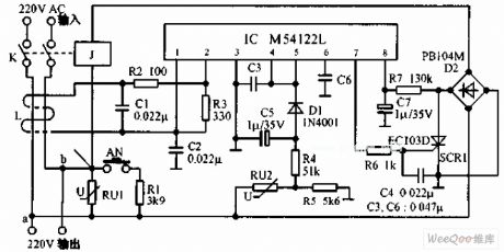
The multi-functional leakage protection switch uses Nissan M54122 which can constitute multifunctional leakage protection switch.The magnetic field is generated by flowing through front line and zero line and it is cancelled out and it does not produce AC current when there are leakage or an electric shock.And coil is produced and 7 feet produces high voltage level,which triggers controlled silicon and makes the relay action cut off power supply. Overvoltage protection is composed of Ru1,Ru2,Ru4,Ru5 and D1.Thermistor Ru1 is used to absorb the overvoltage caused by lightning or center line fault. (View)
View full Circuit Diagram | Comments | Reading(560)
Voltage Generating Circuit with Temperature Compensation
Published:2011/7/19 11:32:00 Author:Michel | Keyword: Temperature Compensation, Voltage Generating Circuit
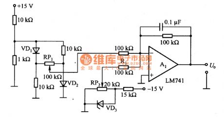
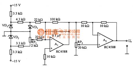
The picture a,b,c are voltage generating circuit with temperature compensation.In the picture (a),VD1 and VD2 constitute temperature sensor circuit and it should generate two positive voltage in order to get the positive and negative temperature coefficient.RP1 sets the voltage temperature coefficient from negative one to postive one.Please regulate RP1 to the left and reduce forward voltage of diode VD2 acording to 2mV/℃ proportion and then use A1 to amplify inversely,which can gain + 2 mV / ℃ voltage.In this state,there is a direct current translation.Thus,the stable benchmark voltage moves the negative output voltge to zero voltage. (View)
View full Circuit Diagram | Comments | Reading(582)
Regulating Circuit of Operational Amplifier and Transistor
Published:2011/7/19 11:22:00 Author:Michel | Keyword: Operational Amplifier, TransistorRegulating Circuit
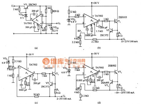

The picture a,b,c,d are regulating circuits of operational amplifier and transistor.The figure (a) is the high stability of operational amplifier output voltage circuit.A1 output uses VDZ1 level shift to make the work stable.VDZ2 is temperature compensation type diode and temperature characteristic is very good. Because the diode current is constant and voltage change is very small. VT1 emitter voltage is about 16V,thus VDZ2 is constant and output voltage is very stable.
Figure(b)~(d) is error amplifier and it uses TA7502 voltage stability circuit.Among them, figure (b) is the circuit whose output voltage is higher than diode stabilizing voltage. (View)
View full Circuit Diagram | Comments | Reading(752)
Regulated Power Supply Circuit with 400V/150mA Output
Published:2011/7/19 11:17:00 Author:Michel | Keyword: 400V/150mA, Regulated Power Supply Circuit
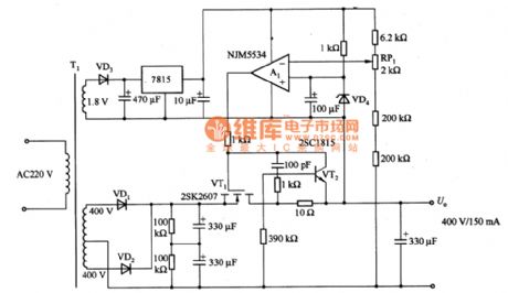
The above picture is regulated power supply Circuit with 400V/150mA output.It is stabilizer of A1 error amplifier of the benchmark voltage (VD4 stable voltage).A1 work power is obtained by voltage of another T1 transformer windings (VD3) and (7815) rectifying and regulating.The circuit adopts over-current protection circuit of characteristics in order to avoid the great loss that produced by the short circuit. (View)
View full Circuit Diagram | Comments | Reading(2233)
The Charger Ciruit of Thyristor
Published:2011/7/19 11:16:00 Author:Michel | Keyword: Thyristor, Charger Ciruit
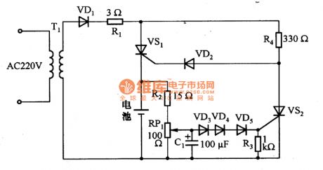
The above picture is the charger circuit of thyristor.This circuit charges nickel battery and the charging current is 1A,The charging time is 1 hour and it stops charging automatically when it is full.Because negative end of nickel-spread battery has negative temperature characteristic,VD3~VD5 forward voltage temperature characteristics compensate for it.When charging battery terminal is low voltage, the voltage on both ends of C1 are also low, thyristor VS2 stops.Thus the current flows through VD1→R1→R4→VD2→VS1 gate→VS1cathode→battery circulation and the power charges battery via VS1.
If the battery voltage rises to the voltage set by RP1, the VS2 triggers and VS1 stops. (View)
View full Circuit Diagram | Comments | Reading(2337)
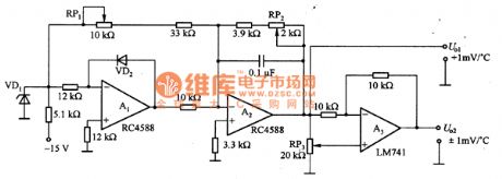
Thermometer of Transistor Temperature Sensor
Published:2011/7/11 7:40:00 Author:Michel | Keyword: Transistor Temperature Sensor, Thermometer
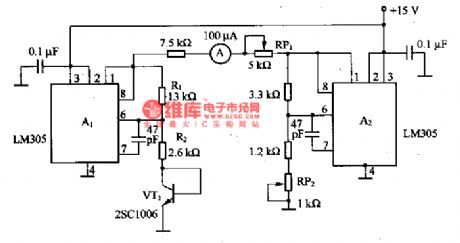
The picture is the thermometer of transistor temperature sensor. In the circuit,VT1 is transistor temperature sensor.A1 uses LM305 as voltage regulation circuit and it provides constant base current for VT1.When LM305 works in the condition that feet 6 feedback input voltage is 1.8V constantly and it is connected to VT1 base and emitter via R2 and Rz keeps the base current constant.R1/R2's change is the change of A1 output voltage.Because there is + lOmV / ℃ temperature characteristics when the output voltage of the LM305 outputs +5V and the same LM305 are used to compensate. The ammeter instruction is 0 if the RP2 is adjusted to -20℃ and the ammeter instruction is 100μA when RP1 is regulated to +80℃. (View)
View full Circuit Diagram | Comments | Reading(1084)
Amplitude Modulation Circuit of Analog Multiplier
Published:2011/7/11 7:39:00 Author:Michel | Keyword: Analog Multiplier, Amplitude Modulation Circuit
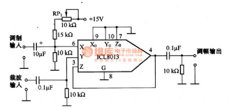
This picture is the amplitude modulation circuit of analog multiplier and it can get amplitude modulation wave through carrier signal and modulation signal multiplication.It can be widely used for general am circuit of low frequency range.ICL8013 is simulation time-multiplier monolithic integrated circuit with +10V input voltage range and it can be used asfour quadrant on time-multiplier and its output voltage,U。=Xy/l0.4 quadrant time-multiplier can be used to balance the modulation and here the bias is fixed which is used to set carrier level when there is no modulation signal.If + 5 V or-5 V bias is imposed ,it can handle + 5 V modulation signal, and then dynamic rangeis extended because handling t voltage is 0 ~ + lOV.The highest carrier signal frequency is 1OOkH and highest voltage of Y input end is 20V.2 OV signal multiplies 5V(X end input voltage) and then they divide 10 to get 10V wave attenuation. (View)
View full Circuit Diagram | Comments | Reading(2485)
Amplitude Modulation Circuit of Analog Switch
Published:2011/7/11 7:37:00 Author:Michel | Keyword: Analog Switch, Amplitude Modulation Circuit
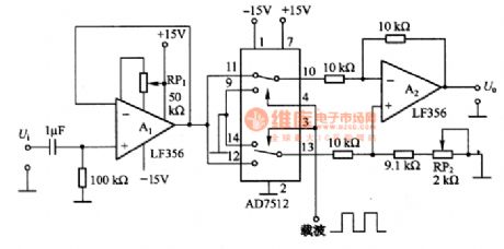
AD7512 and differential amplifiers A2 are used to complete the work. The carrier controls simulation switch and switch contact is connected to the upward side and it inputs via A2 inverse end.The modulation wave is reversed and it returns to normal phase when the next carrier wave comes and the process repeats again and again to achieve the purpose of modulation amplitude limit.It will not stop becuase of carrier cycle but only causes reversal polarity.Analog switch needs to keep up with the carrier frequency, but analog switch frequency can't be high, so the circuit can not be used in high frequency.Modulation output contains the higher harmonic square wave signal and bandpass filter should be added to get the sine wave signal. (View)
View full Circuit Diagram | Comments | Reading(1500)
| Pages:361/471 At 20361362363364365366367368369370371372373374375376377378379380Under 20 |
Circuit Categories
power supply circuit
Amplifier Circuit
Basic Circuit
LED and Light Circuit
Sensor Circuit
Signal Processing
Electrical Equipment Circuit
Control Circuit
Remote Control Circuit
A/D-D/A Converter Circuit
Audio Circuit
Measuring and Test Circuit
Communication Circuit
Computer-Related Circuit
555 Circuit
Automotive Circuit
Repairing Circuit