
Index 362
0-12V Adjustable Voltage Stabilization Circuit
Published:2011/7/17 10:27:00 Author:Michel | Keyword: Voltage Stabilization Circuit
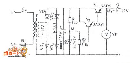
The 0-12 V adjustable voltage stablization circuit is shown as above.Welcome to download the circuit and the information is from www.dzsc.com. (View)
View full Circuit Diagram | Comments | Reading(1021)
CXA1262N Monolithic Record and Play Integrated Circuit
Published:2011/7/19 10:42:00 Author:Michel | Keyword: Monolithic, Record and Play, Integrated Circuit
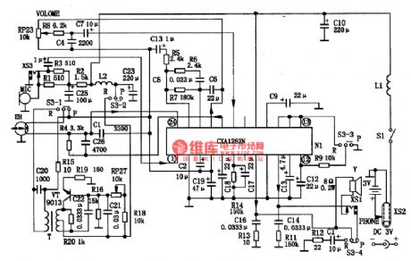
CXA1262N monolithic record and play integrated circuit shown as picture 1 is produced by Sony which is mainly used in pocket recorder.
First CXA1262N Typical Application Circuit.In the circuit,MIC is outside record microphone and VT,T are super audio oscillating circuits. R27 is used to adjust the circuit oscillation frequency. S3 switch is for record/play conversion switch: R23 is to adjust the volume.
Second Signal Flowing Circuit(1) Playback It's in playback situation when S3 is on the position of P.The head loot signal enters the CXAl262N (24) feet and it outputs from (21) feet after preamplifier and frequency compensation. (View)
View full Circuit Diagram | Comments | Reading(432)
PDIUSBD12 Chip Feature and 51 Singlechip Interface Circuit
Published:2011/7/13 8:32:00 Author:Michel | Keyword: Chip Feature, 51 Singlechip, Interface Circuit
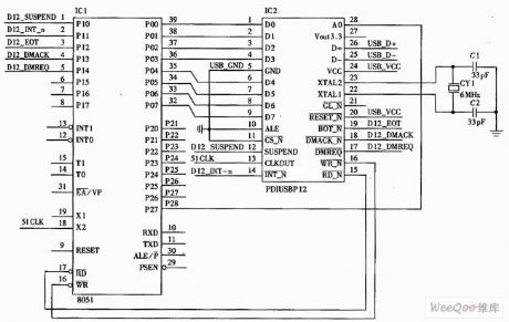
PDIUSBD12 is a performance optimization USB device, usually used in the system based on micro controller. It communicates through the general parallel interface and micro controller and supports local DMA transmission.This device realizes USB interface by using modules and it is allowed to choose the most appropriate micro controller in many micro controllers and it is allowed to use existing micro controller to minimize the devices investment.This flexibility reduces the development time, costs and risks.This device develops an effective way for low cost and high efficiency USB peripherals.
(View)
View full Circuit Diagram | Comments | Reading(857)
LED Power Level Indicator Circuit of LM324 Design
Published:2011/7/12 3:28:00 Author:Michel | Keyword: LM324 Design, LED , Power Level, Indicator Circuit
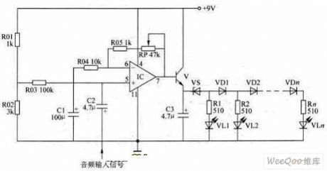
This paper introduces two LED level indicator circuits composed of LM324. The LED level indicator are often applied to audio power amplifier circuit and output power level inductor of power-amplifying circuit. LM324 is four operational Intergrated circuit.
Fitst,the LED PWL inductor introduced firstly has adjustable gain amplification level.It can be connected to audio power amplifier output terminal and also be used as power output level instruction and it could also be connected to the audio preamplifier output terminal (volume control circuit) which is used as prestage indicator.The circuit is showm as above. (View)
View full Circuit Diagram | Comments | Reading(2614)
Nipper Shape Current Transformer
Published:2011/7/11 22:56:00 Author:Michel | Keyword: Current Transformer

SP is serial nipper shape current transformer is one kind of high accuracy current transformer.It can be used with various testing instruments, such as: multi-function watt-hour meter, recorder, oscilloscope, electric power analyzer, digital multimeter, etc .It can measure all kinds of electric parameter when the tested circuit is not cut off.SP series nipper current transformer specification has complete specifications.Users can select proper nipper current transformer according to different occasions and need.
This transformer is our newest research products.It gets consistent high praise from new and old customers since it enters the market.
Welcome to download and the news is from www.dzsc.com. (View)
View full Circuit Diagram | Comments | Reading(610)
Capacitance Driving Circuit with Filter Unit
Published:2011/7/11 22:55:00 Author:Michel | Keyword: Capacitance Driving Circuit
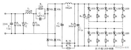
C1, R1, RV1, L1 and R2 constitute the first level power R2 filter circuit, which is used to the input transient momentary high voltage filter.C2, R3 constitutes step-down circuit, C3, C4, L2 and RV2 use rectifying filter circuit.This circuit is double filter circuit and can effectively protect LED from being broken down momentary high voltage.
Picture:Capacitance Driving Circuit with Filter Unit (View)
View full Circuit Diagram | Comments | Reading(480)
DC-DC Conversion Circuit Without Isolation
Published:2011/7/11 22:55:00 Author:Michel | Keyword: DC-DC Conversion Circuit
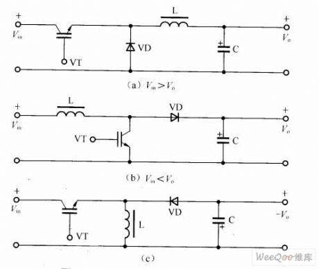
The converter composed of one job switches and L, D, C without input and output voltage isolation and it has three basic forms,namely,buck converter,boost converter and buck-boost converter.And its circuit principle is showed as the aboved pictures.
First,Buck ConverterAs shown in figure (a), 9 is to reduce output ripple, it accesses inductance and capacitance C L on the output side.VD is fly-wheel diode.Output voltage's average value,Vo of buck converter is always lower than Vin. Whether the current iL in inductance is successive depends on switch frequency,filtering inductance L and capacitance C parameter value. (View)
View full Circuit Diagram | Comments | Reading(594)
Single End Forward DC-DC Converter Circuit
Published:2011/7/11 22:55:00 Author:Michel | Keyword: DC-DC Converter Circuit
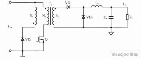
The single end forward DC-DC coverter circuit is showed as above.Among them, the transformer T1 acts as isolation and tranformation and an inductance Lo(flow current inductance) is added to output end,which acts as energy storage and transmission.The transformer primiray level has reset windings Np.In practical applications, the winding uses RCD to absorb can also be replaced.If the chips' auxiliary power supply is provided in the flyback way and part of the adjustable tube peak voltage can also be cutted(It is equivalent to part of the reset winding).Output loop needs a rectifier diode VD1 and a free-wheeling VD2 diode.Transformer uses magnetic cores without the gap thus the copper loses and temperature rising are small and output ripple voltage is small too. (View)
View full Circuit Diagram | Comments | Reading(891)
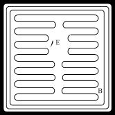
ZIVA-4.1 DVD decoding processing integreated circuit diagram
Published:2011/7/16 2:45:00 Author:leo | Keyword: Decoding processing integreated circuit, DVD devices
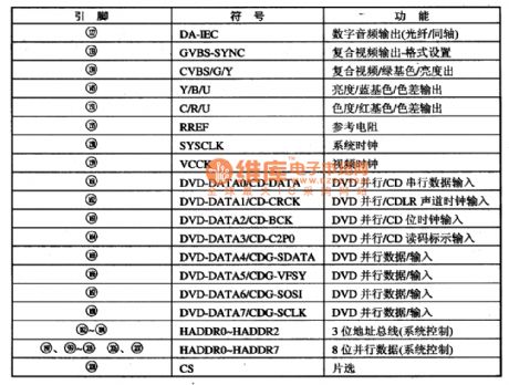
ZIVA-4.1 is a new type of DVD decoding processing integrated circuit. It is widely used in all kinds of DVD devices, for example, BuBuGao series in China and so on.
1.Function Features:The ZIVA-4.1 is used to decode the signals which are from chips and pass through UDE interface circuit. It returns the signals to analog video signals and audio signals. And the analog video signals pass through decoding chip ZIVA-4.1 directly. Audio signals are sent to audio D/A converter and output 5.1 channel analog signals, which are filtered then output.
2.Pin functions and data:ZIVA-4.1 adopts 208 pin package and all functions are shown in the picture. (View)
View full Circuit Diagram | Comments | Reading(618)
MC68HCO5C4-Communication single chip micro computer integrated circuit
Published:2011/7/16 2:45:00 Author:leo | Keyword: single chip micro computer, 24 dual-orientation
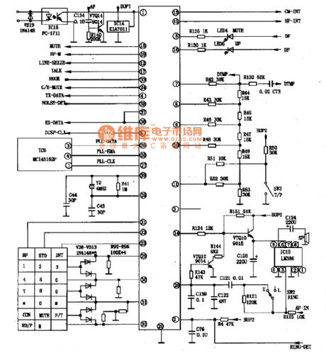
MC68HCO5C4 is a kind of single chip micro computer which is widely used in wireless telephone and always be used as thecontrol chip of main engine.1. Inner circuit diagramMC68HCO5C4 adopts CMOS and has 16 bit input snapping and output comparing self-timer system(IC/OC), constant connecting periphery interface SPI, constant connecting communication interface SCI, 24 dual-orientation input and output line, that is AO-PA7, PBO-PB7, PCO-PC7.
2.MC68HCO5C4 can finish 16 bit snapping and output comparing self-timer system. It can also use output comparing function to generate dual-sound multi-frequency DTMF signals, code data signals, impulse dialing signals, gentle tone and so on. (View)
View full Circuit Diagram | Comments | Reading(589)
Common White LED Driving Circuit
Published:2011/7/13 8:25:00 Author:Michel | Keyword: White LED, Driving Circuit
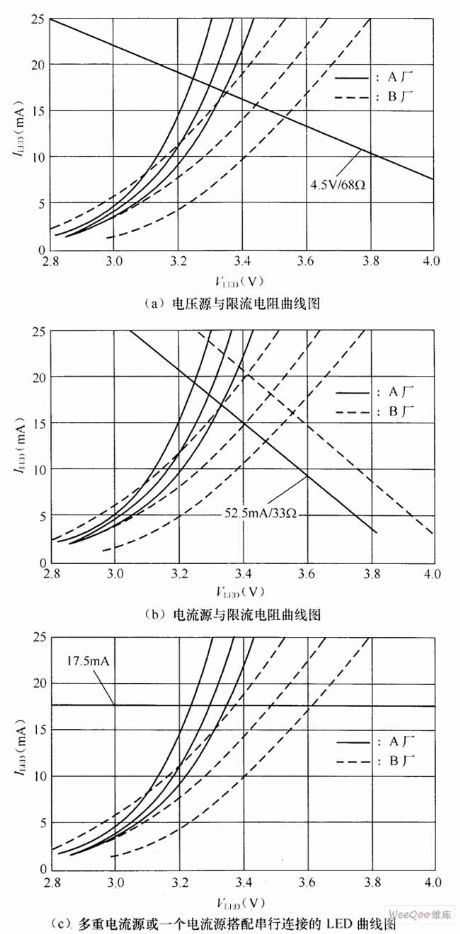
Figure 1 is 4 kinds of common white LED drive circuit and the white LED positive voltage differences will make different impacts to current stable accuracy because different stabilized voltage lines are used. The firgure 2 are six white LED(They are chosen from two manufactuers) positive electric current and forward voltage characteristic curve and , the output voltage stabilizer load curve and lies at the intersection of voltage characteristic curve is the point.
Figure 1: Common White LED Driving Circuit
Circuit shown in figure 1(a) uses voltage source converter and the current limit resistance to control the current white LED and the advantages of the way is that we can choose many kinds of regulators and meanwhile only one end of regulators are connected to white LED. (View)
View full Circuit Diagram | Comments | Reading(609)
A window comparator circuit made by LM311
Published:2011/7/16 2:52:00 Author:leo | Keyword: A window comparator circuit, single polarity voltage
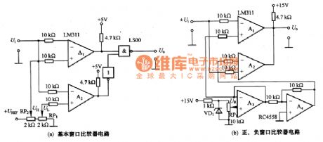
What picture a and b showare a window comparator circuit made by LM311. The picture 14(a) shows a basic comparator circuit input terminal is connected to not-gate window comparator circuit. Input terminal Ui only permits single polarity voltage. When input voltage Ui is lower than the minimum set value UL of window, output high voltage A1 and output low voltageA2 . If the input voltage Ui is higher than UL but lower than UH(maximum), A2 output voltage and the voltage is phase reversalled when passing through inverter. After that, the reversal voltage passes through not-gate phase outputting low voltage which can give a description of the coverage of the window. (View)
View full Circuit Diagram | Comments | Reading(3081)
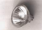
AD521 Solar Lawn Lamp IC
Published:2011/7/13 7:39:00 Author:Michel | Keyword: Solar, Lawn Lamp, IC


AD521 is special IC which is a specially designed for solar LED lighting devices.It consists of switch type circuit, light switch circuit, overdischarging protection circuit, internal integration schottky diodes of circuits, etc.Only an external inductance can constitute solar illumination devices.AD521 uses the patent technology which LED do not glitter when it is off because of undervoltage.
(View)
View full Circuit Diagram | Comments | Reading(546)
Anti-jamming Circuit Principle Diagram with Four Analog Input Channels
Published:2011/7/12 3:32:00 Author:Michel | Keyword: Analog Input Channels, Anti-jamming Circuit, Principle Diagram
Switch input/output channels and analog input and output channels and they are interference enter channels.The object and input/output public ground lines should be removed and interference pulse should be suppressed by realizing electrical isolati to cut off this channel.The most common isolation device is photoelectric couplers, its internal structure is shown as the above picture.
Anti-jamming Circuit Principle Diagram with Four Analog Input Channels
We have to notice that:When we use photoelectric couplers to isolate input output channel,all signals(digital quantity signals,control signal,condition siganl) should be isolated and it makes both sides isolation have no electrical ties.Otherwise,the isolation is meaningless.
(View)
View full Circuit Diagram | Comments | Reading(1341)
Transistor DC/DC Converter Circuit
Published:2011/7/13 8:24:00 Author:Michel | Keyword: DC/DC Converter Circuit
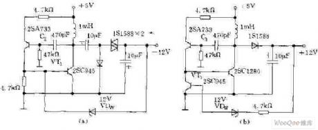
The above picture is a small power DC/DC converter circuit composed of transistor.Picture (a) is the circuit which turns +5V input voltage to -12V output voltage.Picture (b) is the circuit which turns +5V input voltage to +12V output voltage.For any circuit,it's feedback to driving transistor VT1 if the output voltage exceeds voltage regulator tube VDw,which keeps stable output voltage.Thus, output voltage is equal to stable voltage of the voltage regulator tube.And the output voltage can be adjusted if the stble voltage is changed.It works if the capacitance C1 value is changed when the circuit does not oscillate.The output current is 15~20mA,voltage stablity is around 5% and the efficiency is 80%~90%. (View)
View full Circuit Diagram | Comments | Reading(3417)
Battery Discharging Control Indication Circuit
Published:2011/7/13 7:24:00 Author:Michel | Keyword: Battery, Discharging Control, Indication Circuit
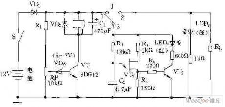
The above picture is battery discharging control indication circuit and its overdischarging circuit is composed of R1,RP and VDw.R3,C2,VT2 and VT3 constitute overdischarging indication circuit.Battery voltage R1 and RP division voltage break down VDw,which make the VT2 getfull and conduct and the 1.3 openning touch point conducts and overlaod R1 works when the switch turns on.R1 and RP can not break down VDw,which can not make VT1 get full and condcut and the relay stops working when the battery voltage decreases to 10~10.5V. (View)
View full Circuit Diagram | Comments | Reading(643)
DC Motor Stepless Speed Governor Circuit
Published:2011/7/13 7:32:00 Author:Michel | Keyword: Speed Governor Circuit
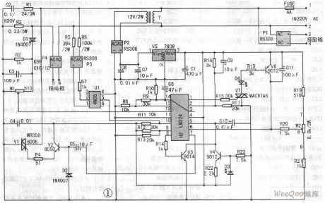
This circuit board circuit is simple, its cost is not high and it is easy to make.The following is simple analysis of the circuit.220 V AC steps down when it flows through transformer T, the P2 rectifier voltage,P2 retifies and V5 constant voltage gets 9V DC voltage and it provides four operational amplifier intergrated chips LM324(Click and Check:four operational amplifier chip LM124 / LM224 / LM324 Chinese material ).P1 rectifier output provides DC motor excitation power supply.P4 rectification gets 0-200V DC by silicon control and realizes motor 0-time speed by connecting motor armature.R1 and C2 are resistance components and they protect controlled silicon. (View)
View full Circuit Diagram | Comments | Reading(1445)
Assembly of the electronic type energy-saving lamp
Published:2011/7/13 23:13:00 Author:TaoXi | Keyword: Assembly, electronic type, energy-saving lamp

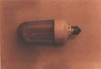
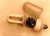

Operating principle: in the moment of the power is connected, the power voltage adds to the two ends of the trigger and light bulb through the ballast, when the light bulb does not light, the circuit is in the open state. The trigger begins to work immediately with the power voltage, and it produces the pulse high voltage that is higher than 3KV to add to both ends of the bulb L, this voltage activates the normal temperature elements of the bulb L into the gas, and the voltage breaks through the gas, L is in the low resistance high current state, so the voltage of the bulb L reduces, it is about 30-50V, the trigger stops working because the voltage is too low. The whole starter process is about 0.8 second.
(View)
View full Circuit Diagram | Comments | Reading(399)
Single Power Complementary and Symmetry Power Amplifier Circuit
Published:2011/7/13 7:21:00 Author:Michel | Keyword: Single Power, Complementary and Symmetry, Power Amplifier Circuit

First,the circuit structure and principleFigure 1 is a circuit uses power complementary and symmetry principle.The T3 constitutes preamplifier stage and T2 and T1 constithute complementaryand symmetry circuit output.When input signal vi=0,usually IC3 ,VB2 and VB1 reach needed value as long as both numerical valueof R1 and R2 are proper.At the time,T2 and T1 are provided a proper offset section,so that the electric potential of K2,VK is equlal to VC and VCC/2.
When the signal vi is added,T1 conducts the electricity ,current flows through load RL and C is charged as the signal is on its negative half cycle.When it's positive half cycle,T2 conducts the electricity,the charged capacitance C acts acts as a double power as power supply -VCC and it discharges via load RL. (View)
View full Circuit Diagram | Comments | Reading(483)
Energy-saving lamps power tube failure mechanism analysis
Published:2011/7/13 23:16:00 Author:TaoXi | Keyword: Energy-saving lamps, power tube, failure, mechanism, analysis
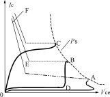
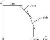
From the failure mechanism analysis, we know that in order to reduce the failure, we need to reduce the operating power of the tube and improve the secondary breakdown characteristic, in fact, the two are related. By the mechanism of the secondary breakdown, we know that the temperature rise increases the tube's HFE and switching performance becomes poor, also the secondary breakdown characteristic; the rise of temperature makes the actual dissipation power parameter become poor, the safe operating area of the tube becomes smaller. vice versa. So in order to improve the quality of the tube, we need to prevent the over-temperature of the tube when it is operating and improve the dissipation power.
(View)
View full Circuit Diagram | Comments | Reading(405)
| Pages:362/471 At 20361362363364365366367368369370371372373374375376377378379380Under 20 |
Circuit Categories
power supply circuit
Amplifier Circuit
Basic Circuit
LED and Light Circuit
Sensor Circuit
Signal Processing
Electrical Equipment Circuit
Control Circuit
Remote Control Circuit
A/D-D/A Converter Circuit
Audio Circuit
Measuring and Test Circuit
Communication Circuit
Computer-Related Circuit
555 Circuit
Automotive Circuit
Repairing Circuit