
Index 376
Current / voltage basic conversion circuit composed of operational amplifier
Published:2011/7/6 7:45:00 Author:Lucas | Keyword: Current conversion , voltage conversion , basic, operational amplifier
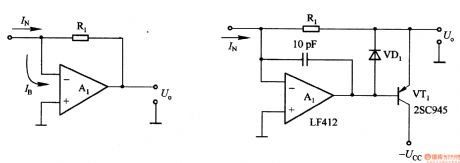
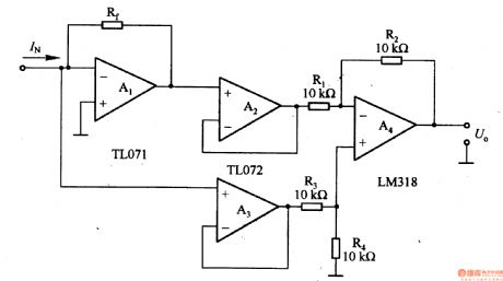
Figure 1-36 (a) shows the current / voltage conversion circuit composed of a single operational amplifier. As the op amp input bias current is not zero, it will produce conversion error. For example, the op amp μA741's bias current IB ≈ 80nA, even if the allowable error is 1%, the minimum switching current is about tens of μA; for Bi-FET input op-amp, IB is about tens of pA, and the minimum switching current is available to a few nA. For the J-FET input op amp, the bias current has a positive temperature coefficient, when the junction temperature increases by 10 ℃, the bias current is increased to 2 times.
(View)
View full Circuit Diagram | Comments | Reading(616)
Voltage / frequency conversion circuit composed of TA7505
Published:2011/7/7 6:13:00 Author:Lucas | Keyword: Voltage conversion , frequency conversion
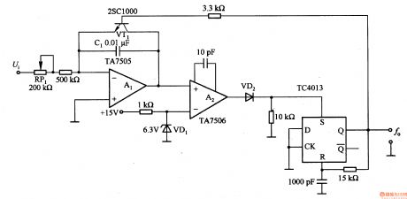
The circuit is composed of the ramp generator, Miller integration circuit, voltage comparator, etc., and it can switch 0-10V input voltage into the corresponding 0-100HZ output frequency. Circuit's switching frequency is determined by the Al ramp generator, and the conversion error is mainly caused by the integrator reset time, dielectric absorption of integration capacitor. In order to reduce errors caused by the reset time, the output of the comparator is connected the trigger composed of TC4013.
(View)
View full Circuit Diagram | Comments | Reading(717)
Voltage / pulse train conversion circuit composed of TC4013
Published:2011/7/7 6:33:00 Author:Lucas | Keyword: Voltage conversion , pulse train conversion
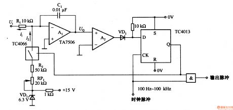
In the circuit, Al is charge-balanced integral amplifier. When UQ <O, the analog switch TC4066 is synchronously disconnected under the rising effect of the of clock, and Al integrates the input voltage Ui, and integral time constant is decided by Rl and Cl, Al output UQ is increased exponentially; When UQ> O, TC4066 is synchronously connected under the effect of clock, and integral circuit makes the reverse integration, and UQ is decreased exponentially; when UQ = O, the integral amplifier is used in combination with the comparator, which is synchronously controlled under the effect of clock to output pulse train which is proportional to input.
(View)
View full Circuit Diagram | Comments | Reading(1893)
Voltage / frequency conversion circuit composed of μA709
Published:2011/7/7 6:40:00 Author:Lucas | Keyword: Voltage conversion, frequency conversion
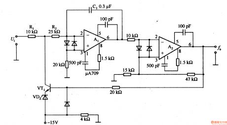
Al integrates the input voltage Ui, and the Schmitt circuit is connected to Al to switch output level and make VT1 saturated conduction. As VTl emitter is clamped by VDZ IN 9V, therefore, VTl collector potential is approximately-9V. Al makes reverse integeration on the voltage, then the output changes from negative to positive, and the time constant is determined by R2 and Cl. If over voltage of Al output is not sensitive, VTl closes again, Al integrates the input voltage again. The circuit swicthes +1 to + lOV input voltage into 0.1 to lkHZ frequency pulse signal.
(View)
View full Circuit Diagram | Comments | Reading(726)
Voltage / frequency conversion circuit composed of μPC157
Published:2011/7/7 6:45:00 Author:Lucas | Keyword: Voltage conversion , frequency conversion
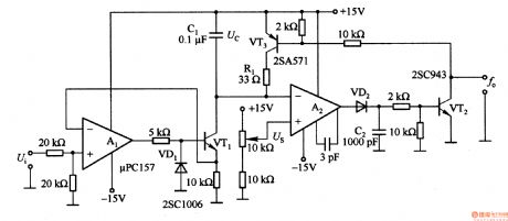
Al is used as voltage / current conversion circuit, which can convert 2V input voltage into lmA current charge for capacitor C1. As the voltage across the capacitor and changes in proportion with the time, so the voltage on the two ends of Cl will be equal the integral value of input voltage and time. A2 is the comparator. When Uc is lower than Us, the output jumps to near + l5V level, the diode VD2 is forward biased to make the transistor VT2 conduction. At the same time, the transistor VT3 is conduction, so the voltage of Uc resets in the constant of Cl and Rl.
(View)
View full Circuit Diagram | Comments | Reading(610)
Voltage / frequency conversion circuit composed of TA7506
Published:2011/7/7 5:45:00 Author:Lucas | Keyword: Voltage conversion , frequency conversion
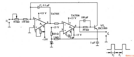
A1 integrates for the input voltage Ui, and the output voltage is applied also to the inverting input, which is compared with the same input reference voltage. If it is less than the reference voltage, A2 outputs high, VT1 turns on, then C1 begins to charge and discharge. The circuit can switch 0-lV voltage signal to 0-10Hz frequency signal.
(View)
View full Circuit Diagram | Comments | Reading(639)
Voltage / frequency conversion circuit composed of FET
Published:2011/7/7 6:00:00 Author:Lucas | Keyword: Voltageconversion, frequency conversion , FET
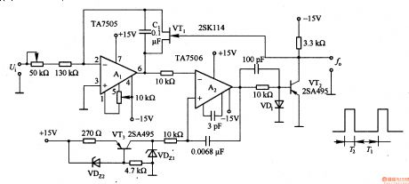
In the T2 period, VTl turns on as the Cl discharge circuit to get a good conversion features. VT3 and VDz2 form the constant current source circuit, which can provide constant current power supply for VDz1. The circuit can switch 0 to -lV voltage signal into 0-10Hz frequency signal.
(View)
View full Circuit Diagram | Comments | Reading(573)
Voltage / frequency conversion circuit composed of LM331
Published:2011/7/7 6:06:00 Author:Lucas | Keyword: Voltage conversion , frequency conversion
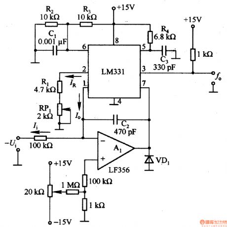
LM331 is the single voltage / frequency conversion IC within 1.9 v reference voltage, current switch, comparator and flip-flop, etc. In order to expand the range, the circuit is added A1 op amp. The reference current IR is decided by (Rl + R (RPl)), as the internal reference voltage is 1.9 V, IR = l · 9V / (Rl + R (RPl)), the usual range is 100 to 500μA. In addition, the current average value of the current switch output (pin 1) end is I. For the internal chip charge-discharge circuit, when the charging voltage reaches 2A as the supply voltage, the circuit is reset.
(View)
View full Circuit Diagram | Comments | Reading(3894)
The basic voltage/frequency conversion circuit composed of transistor
Published:2011/7/7 4:25:00 Author:Lucas | Keyword: basic , voltage conversion, frequency conversion , transistor
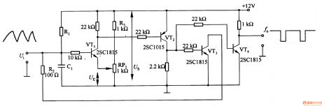
In the circuit, the RlC1 time constant and timing time of control comparator VT1 output are decided by changing set voltage UE. When VTl is turned on, VT2 and VT3 are turned on, then the integration capacitor C1 begins to discharge. R2 can adjust the discharge time constant. When set voltage UE is small, the oscillation frequency increases. In the circuit, VTl, VT3 and VT4 use 2SCl815 or 2SC945, VT2 uses 2SAlO15 or 2SA952.
(View)
View full Circuit Diagram | Comments | Reading(735)
Voltage / frequency conversion circuit composed of LM311
Published:2011/7/7 5:05:00 Author:Lucas | Keyword: Voltage conversion, frequency conversion
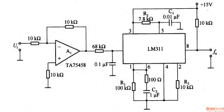
LM311 is the integrated chip within reference voltage, comparator circuit, amplifier, discharge circuit, and it is easy to use. In the circuit, the output frequency f0 is
(View)
View full Circuit Diagram | Comments | Reading(6626)
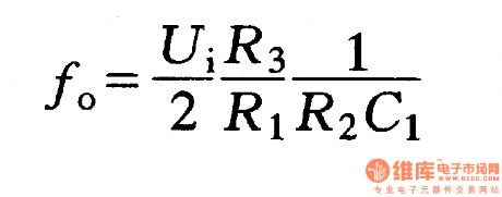
Voltage / frequency conversion circuit composed of two op amps
Published:2011/7/7 5:33:00 Author:Lucas | Keyword: Voltage conversion , frequency conversion , two , op amp
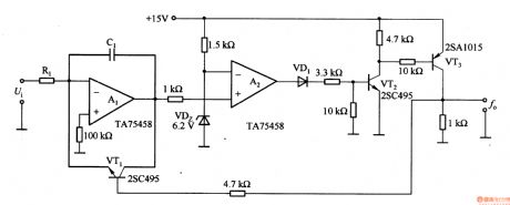
Among them, the operational amplifier Al is integral circuit, and operational amplifier A2 is the comparator circuit; transistor VTl for the discharge circuit. In the circuit, VT1 and VT2 use 2SC495, and VT3 uses 2SAlO15, operational amplifiers Al and A2 use TA75458. Output frequency fo ≈ Ui / (RlClU2), where, U2 is the regulator VDz is regulated voltage.
(View)
View full Circuit Diagram | Comments | Reading(605)
Voltage / frequency conversion circuit composed of M51207
Published:2011/7/7 22:03:00 Author:Lucas | Keyword: Voltage conversion , frequency conversion
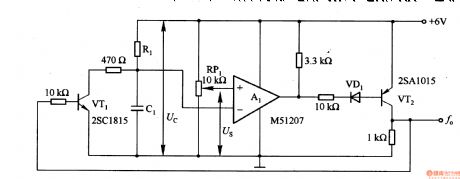
The circuit setting voltage Us has a wide range, and environmental temperature has no effect on it. Voltage / frequency conversion method is used as analog circuit and digital circuit.
(View)
View full Circuit Diagram | Comments | Reading(535)
Voltage / frequency conversion circuit composed of μA741
Published:2011/7/7 21:52:00 Author:Lucas | Keyword: Voltage conversion , frequency conversion
In the circuit, the AI and Rl, R2, Cl, etc. constitute a Miller integrator. Al's triangle wave output can drive level for the comparator. As the clamping effect of VD2, A2 outputs high level in about 0.7 V, low level in about -6V. A2's noninverting input added the feedback voltage is about half of the output voltage, so the upper trip point is about +0.3V, the lower trip point is about -3V. Al outputs triangle wave which is back and forth between +03 to -3V. When A2 outputs low level, VT1 gate voltage is negative and cut-off, R1 + R2 and C1 integrate on 2/3Ui.
(View)
View full Circuit Diagram | Comments | Reading(708)
μPC317H series of regulator, main features and pin of DC-DC circuit and power monitor
Published:2011/7/9 8:02:00 Author:Lucas | Keyword: regulator, main features, pin , DC-DC circuit , power monitor
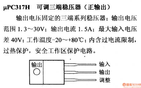
μPC317H adjustable regulator(positive output)
It is the three-terminal regulator with fixed output voltage; output voltage range is 1.3 ~ 30V; output current is 1.5mA; the maximum difference of input voltage is 40V; operating temperature is -20 ~ +80 ℃; it includes over-current limit, thermal protection, protection circuit in safe working area.
(View)
View full Circuit Diagram | Comments | Reading(718)
μPC2600H series of regulator, main features and pin of DC-DC circuit and power monitor
Published:2011/7/9 8:16:00 Author:Lucas | Keyword: regulator, main features, pin , DC-DC circuit , power monitor
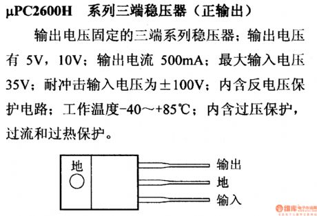
μPC2600H series of regulator ( with positive output)
It is the three-terminal regulator with fixed output voltage; output voltage is 5V, 10V; output current is 500mA; maximum input voltage is 35V; impact resistance input voltage is ± 100V; it contains anti-voltage protection circuit; operating temperature is -40 ~ +85 ℃ ; it includes overvoltage, overcurrent and overtemperature protection.
(View)
View full Circuit Diagram | Comments | Reading(357)
μPC2400HF series of regulator, main features and pin of DC-DC circuit and power monitor
Published:2011/7/9 8:26:00 Author:Lucas | Keyword: regulator , main features , pin , DC-DC circuit , power monitor
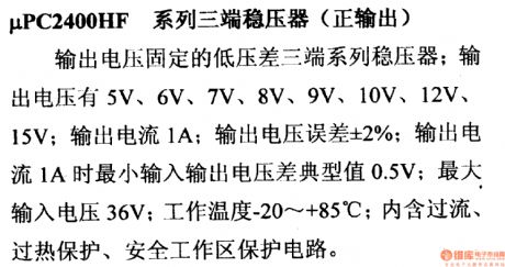
μPC2400HF series of three-terminal regulator ( positive output)
It is the four-terminal low dropout series of regulator with fixed output voltage; output voltage is 5V, 6V, 7V, 8V, 9V, 10V, 12V, 15V; output current is 1A; output voltage error is ± 2%; when output current is 1A, the minimum typical value of difference between input and output voltage is 0.5V; maximum input voltage is 36V; Operating Temperature is -20 ~ +85 ℃; it contains overheat protection, protection circuit in safe operating area.
(View)
View full Circuit Diagram | Comments | Reading(452)
μPC2260H series of regulator, main features and pin of DC-DC circuit and power supply monitor
Published:2011/7/9 7:35:00 Author:Lucas | Keyword: regulator, main features , pin , DC-DC circuit , power supply monitor
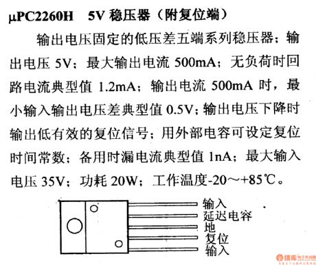
μPC2260H series of regulator ( with reset end)
It is the five-terminal low dropout series of regulator with fixed output voltage and output voltage in 5V; the maximum output current is 500mA; typical value of no-load circuit current is 1.2mA; output current is 500mA, the typical value of maximum input voltage is 0.5V; when output voltage drops, it outputs low signal; external capacitor can set reset time constant; typical value of standby leakage current is 1nA; maximum input voltage is 35V; the power consumption is 20W; operating Temperature is -20 ~ +85 ℃.
(View)
View full Circuit Diagram | Comments | Reading(286)
μPC2250H series regulator,main features and pin of DC-DC circuit and power supply monitor
Published:2011/7/9 7:20:00 Author:Lucas | Keyword: regulator, main features , pin, DC-DC circuit , power supply monitor
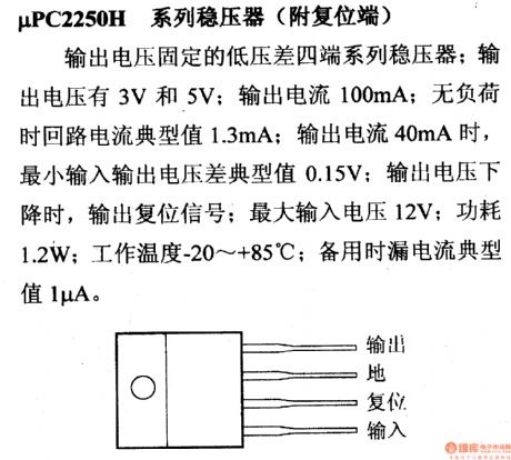
μPC2250H series regulator(with reset end)
It is the four-terminal low dropout series of regulator with fixed output voltage; the output voltage is 3V and 5V; output current is 100mA; typical value of no-load circuit current is 1.3mA; when output voltage drops, it outputs reset signal; maximum input voltage is 12V; power consumption is 1.2W; operating Temperature is -20 ~ +85 ℃; typically value of standby leakage current is 1μA.
(View)
View full Circuit Diagram | Comments | Reading(577)
μPC16300 series of regulator, main features and pin of DC-DC circuit and power supply monitor
Published:2011/7/9 23:30:00 Author:Lucas | Keyword: regulator, main features , pin, DC-DC circuit, power supply monitor
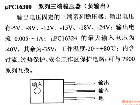
μPC16300 series of three-terminal regulator( with negative output)
It is the three-terminal regulator with fixed output voltage; output voltage can be -5V,,-8V,-12V,-15V,-18V,-24V; output current is 0.005 ~ 1A; maximum input voltage of μPC16324 is -40V, and the rest is -35V; Operating Temperature is -20 ~ +85 ℃; it includes overcurrent, overtemperature protection, safe operating area protection circuit; it can be interchangeable with the 7900 series.
(View)
View full Circuit Diagram | Comments | Reading(519)
μPC14300 series of regulator, main features and pin of DC-DC circuit and power supply monitor
Published:2011/7/9 23:37:00 Author:Lucas | Keyword: regulator, main features , pin , DC-DC circuit , power supply monitor
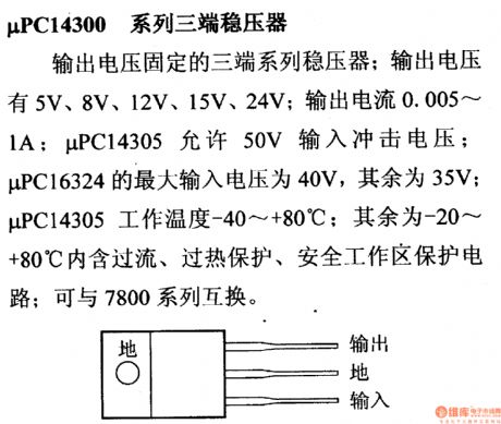
μPC14300series of three-terminal regulator
It is the three-terminal regulator with fixed output voltage; output voltage can be 5V, 8V,12V,15V, 24V; output current is 0.005 ~ 1A; maximum input voltage of μPC14305 is 40V, and the rest is 35V; Operating Temperature is -40 ~ +85 ℃; it includes overcurrent, overtemperature protection, safe operating area protection circuit; it can be interchangeable with the 7800 series.
(View)
View full Circuit Diagram | Comments | Reading(528)
| Pages:376/471 At 20361362363364365366367368369370371372373374375376377378379380Under 20 |
Circuit Categories
power supply circuit
Amplifier Circuit
Basic Circuit
LED and Light Circuit
Sensor Circuit
Signal Processing
Electrical Equipment Circuit
Control Circuit
Remote Control Circuit
A/D-D/A Converter Circuit
Audio Circuit
Measuring and Test Circuit
Communication Circuit
Computer-Related Circuit
555 Circuit
Automotive Circuit
Repairing Circuit