
Index 363
The applications of the full-bridge driver UBA2030T
Published:2011/7/13 23:17:00 Author:TaoXi | Keyword: applications, full-bridge, driver
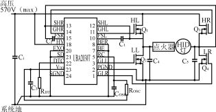
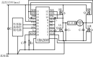
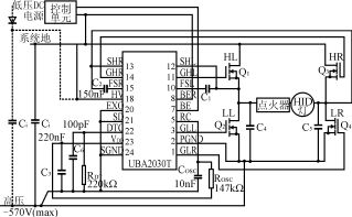
The PHILIPS company uses the BCD750 power logic process method to produce the UBA2030T, this device is designed as one kind of high-voltage IC that can be used to drive the power MOSFET of the full-bridge topology structure. The UBA2030T only needs to use a small amount of the external components to form the high strength discharge (HID) lamp electronic ballast circuit, and it supplies the solution for the design of the HID lamp driving circuit.
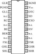
The UBA2030T uses the 24-pin SO package which is as shown in figure 1.
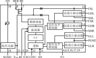
The UBA2030T is composed of the bootstrap diode, the oscillator, the high-voltage and low-voltage electrical level phase shifter, the high-end and low-end drives and the control logic circuit. The internal structure block diagram is as shown in figure 2.
(View)
View full Circuit Diagram | Comments | Reading(823)
Boost DC-DC Converter Circuit of HS7076
Published:2011/7/13 8:23:00 Author:Michel | Keyword: DC-DC, Converter Circuit
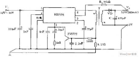
The transformer coupling DC-DC converter shown in the picture is composed of HS7076.The converter's input voltage,output voltage and output current are 15-30V,50V and 300mA respectively.When the circuit works normally, stabilizer conducts,primary transformer flows through current and stores energy,subprime voltage make rectifier diode stop.At the time,output capacitance C discharges to load and the primary electroless diode of transformer stops when the regulator stops. (View)
View full Circuit Diagram | Comments | Reading(552)
Doppler Microwave Automatic Switch Circuit
Published:2011/7/13 7:17:00 Author:Michel | Keyword: Doppler Microwave, Automatic Switch Circuit
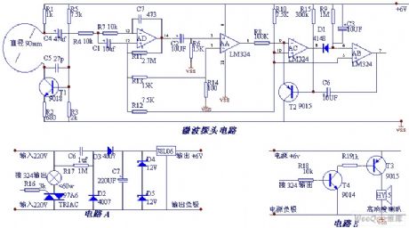
Microwave automatic switch controls the circuit according to microwave doppler effect and it can monitor moving objects and change the moving into electrical signals to control the electric light bulb or electronic appliances opening and closing.
Working principle is same as the following oscillating circuit composed of antenna,T1 and C5.The antenna radiates to the space and it produces a microwave field radius if someone or object in microwave field, which will cause the mobile microwave frequency with about 10 m radius.It will causes microwave frequency shift if someboday or some object moves in the field.In the circuit,it embodies in the change of the voltage of the antenna, C4 will couple this change to the op-amp AD amplification, op-amp output AD forms voltage on R6, when it flows through C2.The voltage's highness and lowliness are relevant to the object distance and moving speed and it's usually between 0-3V.Op-amp AA connects to comparator,it's 0.4V when the reference voltage is 12V. (View)
View full Circuit Diagram | Comments | Reading(2240)
Threshold Switch Circuit of TCAl05 or TCA205A
Published:2011/7/13 7:07:00 Author:Michel | Keyword: Threshold, Switch Circuit
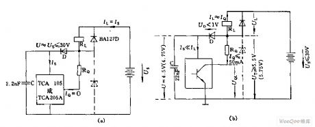
Shown as the above picture,the highest voltage of circuit (a) has risen to 30V from Us=4.5V(When TCA105 is used) or 4.75 (When TCA205A is used).
Here load is relay coil.The load current is 3mA in blocking state and it's load currentinconducting state,. (View)
View full Circuit Diagram | Comments | Reading(893)
Wireless Security Alarm Circuit of 2051 Design
Published:2011/7/11 7:57:00 Author:Michel | Keyword: Wireless Security, Alarm Circuit
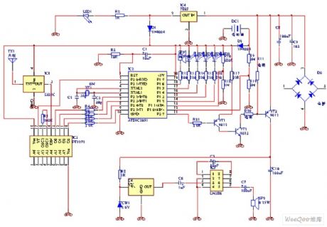
This site to introduce net friend about the core production of wireless security alarm system. The single chip AT89C2051 is used as the central processing chip , which makes the system extension become more convenient.Corresponding soft should be changed if some settings need be altered.This is useful for single chip study.
First,Hardware Design
The circuit principle diagram is shown as above, and it consists of the main wireless access, data decoding, data processing, alarm circuit, output power,alarm display and power supply circuit.The machine receiving frequency is 315M and decoding data uses PT2272 special decoder chip with stable and dependable performance which is widely used in the market.Data processing is completed by the single chip and it is used to distinguish alarm signal,accept all operating instructions and complete the corresponding operation.
(View)
View full Circuit Diagram | Comments | Reading(1607)
PH meter probe amplification circuit diagram
Published:2011/7/21 2:29:00 Author:Ecco | Keyword: PH meter probe , amplification circuit
View full Circuit Diagram | Comments | Reading(3637)
Party line telephone switching equipment 1
Published:2011/7/20 21:32:00 Author:Ecco | Keyword: Party line telephone , switching equipment
View full Circuit Diagram | Comments | Reading(480)
Winder electronic counter circuit diagram 1
Published:2011/7/21 2:50:00 Author:Ecco | Keyword: Winder electronic counter
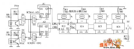
The winder electronic counter circuit is composed of the photoelectric sensor circuit, shaping circuit, plus / minus identification circuit and four-digit counter circuit, and the circuit is shown as the chart. Photoelectric sensor circuit consists of resistors R1, R2, R8, R9 and optocouplers VLC1, VLC2. R1, R8 and VLC1 form the plus counting sensor circuit, and R2, R9 and VLC2 form the subtraction counting sensor circuit. Shaping circuit consists of D1 ~ D4 which are inside of six NOT gate Schmitt trigger integrated circuit IC1.
(View)
View full Circuit Diagram | Comments | Reading(844)
Winder electronic counter circuit diagram 2
Published:2011/7/21 2:53:00 Author:Ecco | Keyword: Winder electronic counter
The winder machine electronic counter circuit is composed of the power circuit, infrared switch circuit, plastic / conversion circuit, reset circuit, divider circuit and LED counter circuit, and the circuit is shown as teh chart. Power supply circuit is composed of the power transformer T, bridge rectifier UR, filter capacitor C4 and three-terminal voltage regulator integrated circuit IC1. Infrared switch circuit consists of infrared light-emitting diode VL, infrared phototransistor V and resistors R1 and R2. Reset circuit is composed of the reset button S1, resistors M, R5 and capacitor C3.
(View)
View full Circuit Diagram | Comments | Reading(1398)
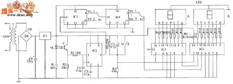
μPCl498H field scanning output circuit diagram
Published:2011/7/21 1:34:00 Author:Ecco | Keyword: field scanning output
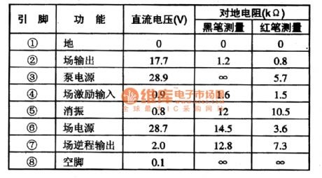
μPCl498H is the new field scanning output integrated circuit produced by Japan NEC, which is widely used in domestic and imported large screen color TV. 1 Features and functionsμPCl498H circuit includes field scanning excitation signal amplifier circuit, field scanning output power amplifier circuit, field scanning pump power supply circuit, vertical blanking pulse generating circuit, and other circuits with auxiliary functions.
(View)
View full Circuit Diagram | Comments | Reading(376)
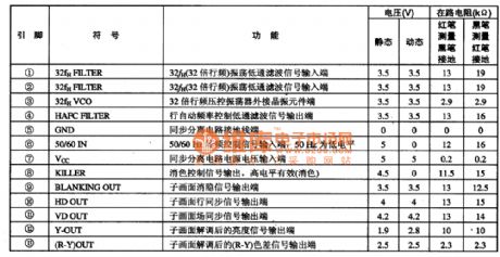
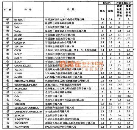
MC141625 - comb filter IC diagram
Published:2011/7/21 1:29:00 Author:Ecco | Keyword: comb filter IC
MC141625 is the comb filter integrated circuit manufactured by Motorola, which is widely used in a variety of domestic and imported color television screen, such as Changhong, 2919 series, TDA series, CN-5 movement and so on. MCI41625 IC uses 48-pin dual in-line package, and the integrated circuit pin functions and data are listed in Table. The measured data in the table is from the 2919 series Changhong color TV . In the actual circuit, the MC141625's pin 19 and pin 42 are grounded wires.
(View)
View full Circuit Diagram | Comments | Reading(659)
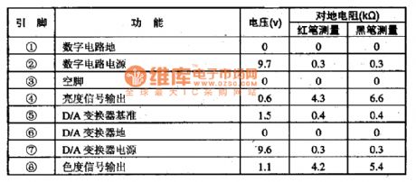
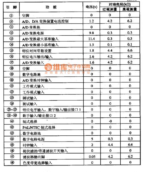
μPC1830GT PIP integrated circuit diagram
Published:2011/7/21 2:02:00 Author:Ecco | Keyword: PIP integrated circuit
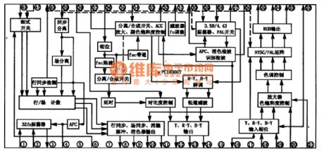
μPC1830GT is the PIP signal demodulation / color demodulation / matrix integrated circuit produced by Japan NEC, which is widely used in domestic and imported large screen color TV. 1. Features and functionsμPC1830GT integrated circuit includes video, chroma, and synchronization processing circuit, and μPC1830GT has PAL and NTSC modem, built-in chroma filter, ribbon-pass filter, luminance delay line and color low-pass filter, and the input signal can be a color video signal or Y / C signal after the separation.
(View)
View full Circuit Diagram | Comments | Reading(784)
MC145151-2 PLL frequency synthesizer circuit diagram
Published:2011/7/21 2:12:00 Author:Ecco | Keyword: PLL frequency synthesizer
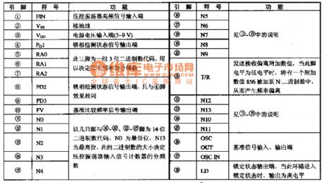
MC145151-2 is the PLL frequency synthesizer IC with dual preset fixed-frequency device. It is suitable for high frequency communications equipment. It has three packages, in order to distinguish by the letter suffix, of which MC145151P-2 is packaged with 28 pin dual in-line package, and MC145151DW-2 is packaged with the 28 pin dual in-line package, and MC145151DW-2 is packaged with the 28-pin package, and MC145151FN-2 is packaged with the SMD ring package. The pin functions are listed in Table.
(View)
View full Circuit Diagram | Comments | Reading(1568)
Voltage follower circuit diagram
Published:2011/7/20 20:11:00 Author:Ecco | Keyword: Voltage follower
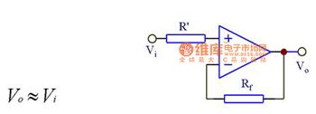
High output resistance and small input resistance can truly transmit input signal to the load, then the signal source currentis low. Voltage follower is a common collector circuit, and the signal is input from the base and output from the emitter, so it is also known as emitter device. Base voltage and collector voltage have the same phase, that is, the input voltage and output voltage is in-phase. The main features of this circuit are: high input resistance, low output resistance, voltage gain is approximately 1, so it is called a voltage follower.
(View)
View full Circuit Diagram | Comments | Reading(643)
The typical application circuit and internal block diagram of LAG668B IC
Published:2011/6/23 2:46:00 Author:Ecco | Keyword: typical application, internal , block diagram , IC
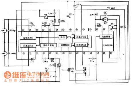
Features of functionLAG668B IC contains two high fidelity pre-amplifier and power amplifier within subwoofer excitation circuit and motor circuit with steady speed. The IC is not combined input capacitor and output coupled capacitor. The block diagram of the circuit and typical application circuit is shown as the circuit. Main electrical parameters The main parameters of LAG668B IC are following:Supply voltage range: 2.3 -4 · 5V, the typical operating voltage is 3V, limit 1 is used as the voltage with 7V.Static current: it is about 18nA. Dynamic operating current: the maximum is 400mA. Because of its large internal resistance, low current, you can get a wide dynamic range both in the case of low and high volume, and the sound quality is good. Power: flat package type is 450mW; dual in-line is 750mW.
The typical application circuit and internal block diagram of LAG668B IC is shown as the chart. (View)
View full Circuit Diagram | Comments | Reading(805)
Four times pressure fluorescent lamp starting circuit diagram
Published:2011/7/20 20:13:00 Author:Ecco | Keyword: Four times , pressure, fluorescent lamp, starting
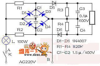
When the A end is positive, B end is negative, the current path is A → L → C2 → D4 → B to make C2 be charged to the peak of electric supply. When the B end is positive, A end is negative, the current path is B → D3 → C1 → L → A to make C1 be charged to the peak of electric supply. At the same time, when A is positive, B is negative, electric supply connected to the voltage on C1 in series will pass D5 to make C3 charge to twice of the peak value; when B is positive, A is negative, electric supply connected to the voltage on C2 in series will pass D6 to make C4 charge to twice of the peak value.
(View)
View full Circuit Diagram | Comments | Reading(516)
The working principle circuit diagram of HT9170
Published:2011/7/20 20:13:00 Author:Ecco | Keyword: working principle
HT9170 will send DTMF signal to the pre-filter (actually a band stop filter) after passing the operational amplifier to filter the 350 ~ 400Hz low frequency interference and noise in DTMF signals. Basically, the output signal contains only two frequencies. The output signals will output high-frequency and low-frequency sine wave signals after respectively passing the two band-pass filters with high-frequency and low-frequency filters, then they will be turned into the rectangular pulses with the same frequency after shaping by the Schmitt circuit.
(View)
View full Circuit Diagram | Comments | Reading(1440)
Digital velocity detection circuit
Published:2011/5/13 3:33:00 Author:Nicole | Keyword: digital velocity detection
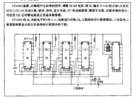
CC4060 oscillation, frequency divider produces standard second signal, to adjust 58kΩ resistance, to make Q9 outputs T=2s square wave(duty cycle is 50%). CL102 completes counting, latch, decoding, display function. RC forms oscillator, but the precision is not high. In demanding occasion, we can use 555 timer circuit or quartz crystal oscillator.
When Q9 of CC4060 is low level(about 1s), the circuit starts to count; when Q9 isjumping, the timer is latched. 4 bits LED displays the number of count pulse per second. (View)
View full Circuit Diagram | Comments | Reading(627)
Random electronic dinky toy circuit
Published:2011/5/13 2:59:00 Author:Nicole | Keyword: electronic dinky toy
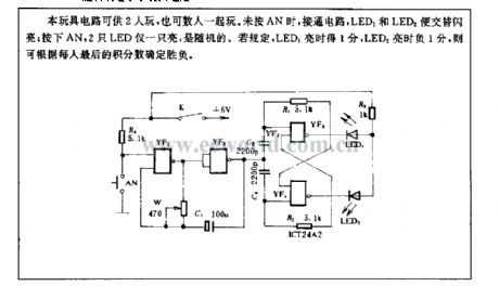
This toy circuit can be played by 2 persons, even more people. If it does not press AN, thecircuit is turned on, LED1 and LED2 is flashing by turns; to press AN, only one of LEDs turns on, it is random. To order if LED1 turns on, it will obtain 1 point, and LED2 turns on, it will obtain negative-one point, the victory or defeat is decided by everyone's final point. (View)
View full Circuit Diagram | Comments | Reading(477)
Bridge luminometer circuit
Published:2011/5/13 2:29:00 Author:Nicole | Keyword: luminometer
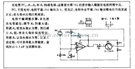
The electric bridge is composed of phototube PC1, R1, R2, R3, differential input terminal of operational amplifier 741 is connected to the middle point of electric bridge both arms.
When PC1 has no light, the electric bridge is balance, 741 output is 0, after it has light, the electric bridge loss balance, 741 output terminal level is directly proportional to the brightness, the meter indicates the brightness value.
The balance adjustment steps of electric bridge: you can shading the phototube at first, adjusting R5 to the maximum value, then adjusting R3 to make the meter indicates 0. To reduce R5, making the meter hand stray away from 0, then adjusting R3 to make the meter indicates 0. To repeat this process, it can obtain the maximum sensitivity. The broken line shows 0.1μF decoupling capacitance. (View)
View full Circuit Diagram | Comments | Reading(751)
| Pages:363/471 At 20361362363364365366367368369370371372373374375376377378379380Under 20 |
Circuit Categories
power supply circuit
Amplifier Circuit
Basic Circuit
LED and Light Circuit
Sensor Circuit
Signal Processing
Electrical Equipment Circuit
Control Circuit
Remote Control Circuit
A/D-D/A Converter Circuit
Audio Circuit
Measuring and Test Circuit
Communication Circuit
Computer-Related Circuit
555 Circuit
Automotive Circuit
Repairing Circuit