
Index 4
Great Wall programmed box fan circuit
Published:2012/11/20 20:34:00 Author:Ecco | Keyword: Great Wall , programmed box fan
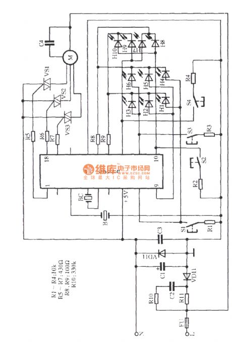
Great Wall FS36-40 fan uses programmable technology, and it has three wind species, three wind speeds and four-time segment timing shutdown function. It also has 10W lights at night, and the circuit is shown as the figure. The circuit uses IC chip RTS-1A with fewer external components and manual operation and automatic operation. H1 ~ H10 are light emitting diodes.
(View)
View full Circuit Diagram | Comments | Reading(1694)
Homemade fast hand dryer circuit
Published:2012/11/20 1:27:00 Author:Ecco | Keyword: Homemade, fast hand dryer

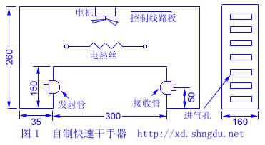

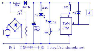
When it is illuminated, the IC's pin 1 is in high potential, TWH8751 is cutoff, J loses power, J1-1 disconnects. When the hand gets into and blocks the light, D2 shows a large resistance, pin 2 of the IC is in a low potential, the IC output end gets conduction, J1-1 is turned on, the electric wire and the motor are energized.
(View)
View full Circuit Diagram | Comments | Reading(1940)
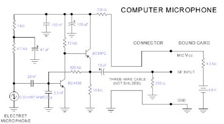
Computer Microphone
Published:2012/11/19 21:41:00 Author:muriel | Keyword: Computer Microphone
View full Circuit Diagram | Comments | Reading(1199)
High Power FM Wireless Microphone
Published:2012/11/14 0:55:00 Author:muriel | Keyword: High Power , FM , Wireless, Microphone
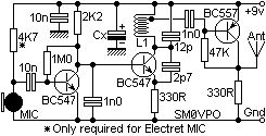
This FM Wireless Microphone has been a very popular project with beginners and experienced constructors alike. It has been used inside guitars and as the basis of a remote control system. I do however, receive many requests for a higher powered circuit and better microphone sensitivity. This High Power FM Wireless Microphone has a better frequency stability, over 1 Km range and is good on microphone sensitivity. This has been achieved by adding an RF amplifier buffer (with 10dB gain) and an AF preamplifier to boost the modulation a little.
Construction is quite simple. L1 is 3.25 turns in spiral form and is an integral part of the PCB foil pattern. The two BC547 transistors can be replaced with (almost) any small-signal NPN transistor, such as the 2N2222. The final stage is a BC557 PNP general purpose device. If you use different devices then you should select the 1M0 resistor for 5-volts DC at the collector of the the first transistor. Select the 47K resistor for 3 � 4 volts on the collector of the third transistor. Here is the V5 component overlay drawing. Note that there is a modification: The PCB is 50mm x 25mm, a little larger than the first version but there are three stages instead of just the one. The first prototype is shown above, beside the battery powering it. The output power is about +10dBm which is about 10dB more than the first FM Wireless Microphone. This would theoretically give it 3.12 times the range (1.6Km) but I have only tested it using a handheld with the TX laying on the bench indoors. But I got a comfortable 700 meters (and a few funny looks from our neighbours). Above you can see the addition of a capacitor added across the 12p tuning capacitor to lower the frequency of the transmitter. Make the capacitor by twisting two lengths of single core insulated hook-up wire, about 2cm long. This will reduce the frequency to the bottom end of the band. Cut short the capacitor to increase the frequency to the desired final frequency. If you cut it a few KHz too high then just twist the gimmick a little tighter. (View)
View full Circuit Diagram | Comments | Reading(1858)
Dual-Voltage Supply Powers SIM Card
Published:2012/11/8 1:07:00 Author:muriel | Keyword: Dual-Voltage, Supply , Powers SIM Card
View full Circuit Diagram | Comments | Reading(1637)
Cellular Telephones/Cameras
Published:2012/11/8 0:51:00 Author:muriel | Keyword: Cellular Telephones/Cameras
View full Circuit Diagram | Comments | Reading(1055)
NORELCO rechargeable electric shaver circuit
Published:2012/10/26 21:41:00 Author:Ecco | Keyword: NORELCO , rechargeable, electric shaver
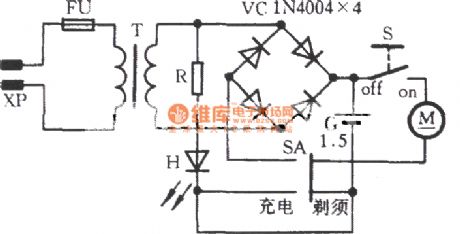
When it is charging, SA is put to charging , after XP is inserted into the 220V power outlet,T's secondary stage is 4V (unloaded), and it is charging for battery after being rectified by VC. Usually, a single charging time is 8-10 hours. H is the charging light which is illuminated when charging. When peopel use ot for shaving, switch SA is turned to shave position, then s is swicthed to on position, M rotary can make shaving. S is switched to off , the machine is turned off.
(View)
View full Circuit Diagram | Comments | Reading(4523)
Simple Op-Amp Radio
Published:2012/10/18 22:46:00 Author:muriel | Keyword: Simple , Op-Amp Radio
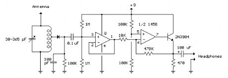
This is basically a crystal radio with an audio amplifier which is fairly sensitive and receives several strong stations in the Los Angeles area with a minimal 15 foot antenna. Longer antennas will provide a stronger signal but the selectivity will be worse and strong stations may be heard in the background of weaker ones. Using a long wire antenna, the selectivity can be improved by connecting it to one of the taps on the coil instead of the junction of the capacitor and coil. Some connection to ground is required but I found that standing outside on a concrete slab and just allowing the long headphone leads to lay on the concrete was sufficient to listen to the local news station (KNX 1070). The inductor was wound with 200 turns of #28 enameled copper wire on a 7/8 diameter, 4 inch length of PVC pipe, which yields about 220 uH. The inductor was wound with taps every 20 turns so the diode and antenna connections could be selected for best results which turned out to be 60 turns from the antenna end for the diode. The diode should be a germanium (1N34A type) for best results, but silicon diodes will also work if the signal is strong enough. The carrier frequency is removed from the rectified signal at the cathode of the diode by the 300 pF cap and the audio frequency is passed by the 0.1uF capacitor to the non-inverting input of the first op-amp which functions as a high impedance buffer stage. The second op-amp stage increases the voltage level about 50 times and is DC coupled to the first through the 10K resistor. If the pairs of 100K and 1 Meg resistors are not close in value (1%) you may need to either use closer matched values or add a capacitor in series with the 10K resistor to keep the DC voltage at the transistor emitter between 3 and 6 volts. Another approach would be to reduce the overall gain with a smaller feedback resistor (470K). High impedance headphones will probably work best, but walkman stereo type headphones will also work. Circuit draws about 10 mA from a 9 volt source. Germanium diodes (1N34A) types are available from Radio Shack, #276-1123. (View)
View full Circuit Diagram | Comments | Reading(1491)
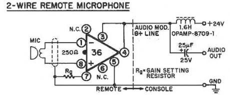
2-wire remote microphone
Published:2012/10/18 3:31:00 Author:muriel | Keyword: 2-wire, remote microphone
View full Circuit Diagram | Comments | Reading(4722)
Auto Bathroom Fan control
Published:2012/10/10 1:55:00 Author:muriel | Keyword: Auto, Bathroom Fan
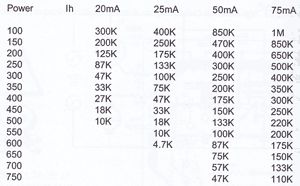
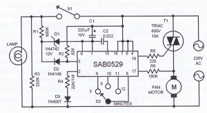
This auto bathroom fan control circuit design is a lamp and fan motor control with a delayed switch off. This automatic fan control is commonly used in toilet and bathrooms. When switch S1 is closed, the fan motor and the lamp turns on. When switch S1 is opened (switched off), the lamp goes out but the fan motor will keep running for another 3, 6 or 1 minutes linger (set by S2). This delayed switching off of the fan ensures that the unwanted odor is really fanned out the toilet.The heart of the bathroom exhaust fan circuit is the SAB0529 IC. It is a programmable extended time timer brought to the market by Siemens. This IC can be programmed to time from 1 second up to 31.5 hours. This extended time capacity is achieved by the IC by using the power line frequency as its time base.
The bathroom fan light control circuit is commonly used to control inductive loads such as the case of fan motor. For this reason, a current synchronization is necessary. This is done with resistor R6. In addition, a capacitor C2 is connected between pins 15 and 1. This capacitor sets the pulse length at the output pin 16. If one decides to use a different triac, one needs to change the value of R5 . THis resistor sets the level of the trigger current, in this case 5 mA. The syc resistor R6 must be changed also. If the triac power and holding current (Ih) are known, one can get the value of R6 from the table below:
bathroom fan controller circuit diagram
(View)
View full Circuit Diagram | Comments | Reading(2643)
PC FM Radio circuit
Published:2012/10/10 1:46:00 Author:muriel | Keyword: PC, FM Radio
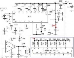
This is a fm radio receiver circuit which can be used with PC.PC radio REGULATIONSA) With the P1 we regulate the intensity of sound.B) With the P2 we regulate the frequency of reception.C) Optionally: If you want to check the frequency with your PC it will be supposed you make the following energies:- You assemble and the circuit that is in the blue frame.- You cut the driver dj’pla in point A, as it appears in the circuit and you connect points A,V.- If you know some language of programming as C ++, PASCAL, VISUAL BASIC, DELPHI etc you can write a program which will send in the parallel door (378 I) of PC a number from 0 until 255 checking thus the tendency of expense of simple D/A of converter (that it is in blue frame) and consequently and frequency of radio via passage VARICAP.(As long as grows the number that sends in the parallel door, so much minimizes the frequency that receives the radio.)Download DOS control program – radio fm pc dosPC FM receiver materials and circuit componentsThe resistances are 1/4W.R1 47KR2 22KR3 100KR4 39KR5 10R6-r12 7,5K – OptionallyR13-r21 15K – OptionallyP1 10K Logarithmic potentiometerP2 100K Linear potentiometerC1 39pF CeramicC2 47pF CeramicC3 2,2nF PolyesterC4, c14 220nF PolyesterC5 22nF PolyesterC6 10nF PolyesterC7, c18 180pF CeramicC8 150pF CeramicC9 100nF PolyesterC10, c13 330pF CeramicC11 220pF CeramicC12, c16 3300pF CeramicC15, c17 1800pF CeramicC19, c21, c22 10mF/16V electrolyticC20 10nF PolyesterC23 47nF PolyesterC24, c25 470mF/16V electrolytic capacitorL1, l2 5 Coils linked with internal diameter 4mm from cupreous isolated wire 0,6mm.IC1 TDA7000 with base DIL18IC2 LM7805IC3 LM386 with base DIL 8D1 BB329 or BB105 or other than old tuner televisions.SPEAKER Loudspeaker 8W/1W.S1 Switch of catering.AERIAL 50cm isolated wireCONNECTOR DB25 Fastener of 25 pin parallel door PC (LPT) -Optional
PC FM Radio circuit diagram
(View)
View full Circuit Diagram | Comments | Reading(3345)
Temperature Controlled DC Fan
Published:2012/10/9 2:31:00 Author:muriel | Keyword: Temperature Controlled, DC Fan
This circuit can cool your heat generating electronic devices by operating a DC fan when the temperature in its vicinity increases above the preset level. Its operation is fully automatic and turns off when the temperature returns normal. It uses a small 12V DC brush less fan used in computersThe circuit exploits the property of Thermistor to operate the DC Fan. Thermistor is a kind of temperature dependent resistor and its resistance varies depending on the temperature in its vicinity. There are two types of Thermistors- NTC and PTC. Negative temperature coefficient (NTC) Thermistor decreases its resistance when the temperature increases while Positive temperature coefficient (PTC) increases its resistance when the temperature increases. Thermistors are bead like resistors available from 100 ohms to 10K or more values. Here a 4.7K NTC Thermistor is used. IC uA 741 is used as a voltage comparator to switch on the DC fan. Its INV input (pin2) gets an adjustable voltage through VR while its Non-INV (pin3) input gets voltage through a potential divider comprising R1 and the Thermistor. Thus the voltage at pin3 depends on the conductivity of the Thermister.
When the temperature is normal (as set by VR), pin3 gets higher voltage than pin2 and makes the output of IC high as indicated by Red LED. This high output keeps T1 off since its base is positive. DC fan remains off in this condition. When the temperature increases above the value set by VR, resistance of Thermister decreases and the voltage at pin3 decreases. As a result, output of IC becomes low to switch on T1. A small brush less DC fan (one used in computers) turns on to increase the air circulation. When the temperature returns normal, Fan automatically turns off. Diode D3 is necessary to remove back e.m.f when T1 turns off. Green LED indicates that the Fan is operating.
DC Fan Controlled by Temperature Circuit Diagram
(View)
View full Circuit Diagram | Comments | Reading(1464)
Pachisi Game Circuit
Published:2012/10/8 2:50:00 Author:muriel | Keyword: Pachisi Game
Pachisi game is designed for two persons. Each player has one figurine; the figurines are found in the early game on positions indicated by arrows. The goal of each figurine is the white square field in the middle of the game. Players move in turn: they need to move the figurines forward or back on the next black or white field. If a player reaches with his figurine on a field that already is occupied by the other player then he wins.4 LEDs indicate if the figure should be moved forward or back, or should be put on the next field white or black. By pressing S1, LEDs indicate by chance, randomly “before” or “back” and “black” or “white”.
The assembly is not complicated: two bistable multivibrators form a binar counter with 2 bits. Leds are used to make visible the counter position; the 4 transistor are sued to power up the LEDs.
Pachisi Game Circuit Diagram
Pachisi Game Table Board
(View)
View full Circuit Diagram | Comments | Reading(931)
Panic Alarm Circuit
Published:2012/9/28 21:05:00 Author:muriel | Keyword: Panic Alarm Circuit
Imagine the Panic situation in the Midnight when an intruder tries to break into the house. This Alarm will help you with its loud Police siren to abort the attempt of intrusion. With a single clap, the circuit generates the alarm for three minutes and then goes off. This is sufficient to catch the attention of neighbours.The circuit is a sensitive Clap switch with timer action. IC1 is designed as a sensitive inverting amplifier to amplify the sound signals from the condenser mic. Variable resistor VR1 set the sensitivity of mic and resistor R1 and VR2 set the gain of the amplifier. If the sensitivity of mic and amplifier is suitably adjusted, the circuit can detect the sound from a distance of 5meters or more.
Panic Alarm Circuit Diagram
(View)
View full Circuit Diagram | Comments | Reading(1189)
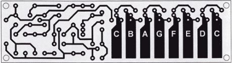
Electronic Organ Circuit
Published:2012/9/27 21:37:00 Author:muriel | Keyword: Electronic Organ
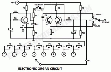
This electronic organ circuit is very simple to construct and is basically an emitter-coupled oscillator composed of T2 and T3. An squarewave voltage can be sampled from the collector of T3 (X2). This signal gives a clarinet character to the tone.Without the squarewave signal, the sound produced by emitters of T2 and T3 (X4) has a violin character. An additional vibrato signal can be added to this basic sound through switch S1. The frequency of the vibrato is around 6 Hz. Its amplitude is determined by the R4. The value of R4 can vary from 100 up to 300KΩ but you can experiment with different values.
The organ keys can be made of either metal plates or etched printed circuit.The trimmers P1 up to P8 adjust the pitch of each tone. The tones can be drastically changed by changing the value of C4.
Electronic Organ circuit diagram
Printed Circuit Board for the Electronic Organ
(View)
View full Circuit Diagram | Comments | Reading(2543)
APR 9301 Voice Recorder
Published:2012/9/27 21:24:00 Author:muriel | Keyword: APR 9301, Voice Recorder
APR 9301 is a single chip Voice recorder and Play back device for 20 to 30 seconds voice recording and play back. It is an ideal IC for automatic answering machine, door phones etc. This IC has data storage capacity and requires no software and microcontroller. It provides high quality voice recording and play back up to 30 seconds.APR9301 Datasheet
The IC requires minimum components to create a voice recorder. The IC has non volatile flash memory technology with 100K recording cycles and 100 year message retention capacity. The IC utilizes the Invox proprietary analog / multi level flash non volatile memory cells that can store more than 256 voltage levels. It requires a single 5 volt supply and operates in 25 mA current.
APR 9301 Voice Recorder Circuit
Mode of operation
1. Record ModeThe LED glows when the IC records the voice obtained through the Mic. A single voice message up to 20 seconds can be recorded. The IC remains in the recorded mode as long as the RecL pin 27 is grounded. Recoding will be terminated with the last memory when 20 seconds is over. The Speaker driver will automatically mutes in the recording mode. By changing the value of the OscR resistor R1 it is possible to increase the recording period as follows
A. R1 52K 20 Sec.B. R1 67 K 24 SecC. R1 89 K 30 Sec.
APR 9301 IC
(View)
View full Circuit Diagram | Comments | Reading(1466)
CD Burner – How the CD Burning is done
Published:2012/9/27 21:23:00 Author:muriel | Keyword: CD Burner
CD burning is an amazing technology and its working principle is really fascinating. CD burners encode music and other datas on to the blank CD which can be retrieved through CD reading. CD stores the datas in digital form represented by a series of 1s and 0s. The 1s are represented by tiny bumps and the 0s as flat areas. Such millions of bumps and flats areas are present in a standard size CD.
A CD is made from 1.2 mm thick, almost-pure Polycarbonate plastic and weighs 15–20 grams. From the center outward components are at the center (spindle) hole, the first-transition area (clamping ring), the clamping area (stacking ring), the second-transition area (mirror band), the information (data) area, and the rim.
A CD is made up of a polycarbonate plastic known as Polymethyle Meta acrylic.The surface of the CD is coated with a thin layer of Aluminium to make it reflective, and is protected by a film of lacquer that is normally spin coated directly on top of the reflective layer, upon which the label print is applied.
The bumps and flat areas are present on the reflective side of the CD which is arranged in continuous tracks. These tracks measures about 0.5 microns and can stretch about 5 Kms. During CD reading, a ‘Read laser beam’ passes over the flat area in the track. The laser beam will reflect back which will be passed onto a photo sensor assembly. The Photo sensor interprets the reflected laser light as 1. When the laser light bounce back from the bumps, the photo sensor will not get it and the CD player recognize it as 0.
Blank CD
The bumps are arranged spirally starting from the centre of the CD to the periphery. The motor in CD player spins the CD in a steady speed. The laser assembly of the CD player moves from the center to the periphery of the CD at a steady speed to retrieve the data. The CD player shows a slow spinning speed as the laser assembly move outwards to keep the bumps moving past the laser at a constant rate. The digital information retrieved by the photo sensor will be then converted into audio or video by the amplifier circuit.
CD burring technique
CD writer is used to burn the CD to record the data in the digital format. The CD burner darkens microscopic areas in the reflective side of the ‘Blank CD’. During burning, both reflective and non reflective areas are created in the CD that can be interpreted as 1 and 0 by the CD player. The CD burner has a laser assembly similar to the CD reader. But the laser is ‘Write Laser’ with high power around 40 mW. The write laser interacts with the CD and alters its surface.
(View)
View full Circuit Diagram | Comments | Reading(1447)
Electronic Cricket Match Game
Published:2012/9/25 1:05:00 Author:muriel | Keyword: Electronic Cricket,Match Game
This electronic cricket is a present for Kids. This simple battery powered circuit can be used to play Cricket Match with your friends. Each LED in the circuit indicates various status of the cricket match like Sixer, Run out, Catch etc.
The Circuit uses two ICs ,one in the Astable mode and the second in the display driver mode. IC1 is wired as an Astable Multivibrator with the timing elements R1, R2 and C1. With the shown values of these components very fast output pulses are generated from the Astable. Output from IC1 passes into the input of IC2 which is the popular Johnson Decade counter CD4017. It has 10 outputs. Of these 8 outputs are used. Output 9 ( pin9) is tied to the reset pin 15 to repeat the cycle. When the input pin 14 of IC2 gets low to high pluses, its output turns high one by one. Resistor R3 keeps the input of IC2 low in stand by state to avoid false indications.
Electronic Cricket Circuit Diagram
When the Push Switch S1 is pressed momentarily, the Astable operates and all the LEDs run very fast sequentially. When S1 is released, any one of the LED stands lit which indicates the status of the match. For example, if LED D7 remains lit, it indicates Sixer and if LED 8 remains lit, it indicates Catch out.
Label each LED for its status as shown in the diagram. Pressing of S1 simulates Bowling and Running LEDs indicates running of Batsman. (View)
View full Circuit Diagram | Comments | Reading(984)
Positive Trigger Timer circuit
Published:2012/9/25 0:52:00 Author:muriel | Keyword: Positive,Trigger,Timer
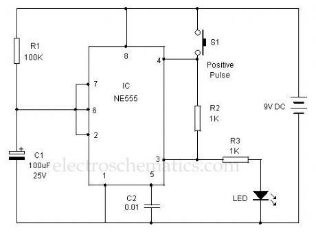
This 555 Timer is designed unusually to give a positive output through a control over its reset pin. Usually the timer IC 555 is triggered by applying a negative going pulse to its trigger pin 2. This timer is triggered through a positive pulse in its reset pin.
In the Monostable mode IC 555 starts timing cycle when a negative pulse is applied to its trigger pin2. The timer starts oscillations only when its trigger pin goes to ground potential. The reset pin 4 is usually connected to positive rail to keep the timer ready to oscillate.
Here an alternate mode of operation is experimented. At power on, the voltage level in the capacitor C1 is less than 1/3 Vcc. This resets the internal Flip-Flop of IC and its output goes high and LED turns on.C1 then charges through R1. When the voltage level in C1 rises to 2/3 Vcc, output of IC turns low and LED turns off. This low output from pin 3 pulls the reset pin 4 to a low state and IC latches to off condition. The latching state continues even if the capacitor C1 discharges through the discharge pin 7 and voltage in C1 drops below 1/3 Vcc.
Positive Trigger Timer circuit
(View)
View full Circuit Diagram | Comments | Reading(3654)
Handy Pen Torch circuit
Published:2012/9/24 4:21:00 Author:muriel | Keyword: Pen, Torch
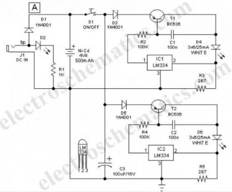
This easy to construct “Handy pen torch” electronic circuit and low component count, uses two power white LEDs for lighting. Low volt (4.8V dc) supply available from the built in rechargeable Ni-Cd battery pack is first converted into two channel (independent) constant current sources by two pieces of the renowned precision adjustable shunt regulator chip LM334 (IC1 and IC2).Around 25 mA at 3.6 volt dc is available at the output of these ICs. This regulated dc supply is used to drive two power white LEDs D4 and D6. Resistors R3 and R5 limlits the output current (and hence the light output) of IC1 and IC2 circuits respectively.Besides these components, one red color LED (D2) is included in the main circuit which works as a battery charging supply input indicator.Resistor R1 limits the operating current of this LED .
Pen Torch Electronic Circuit Schematic
Diode D1 works as an input polarity guard cum reverse current flow preventer. Capacitor C1 is a simple buffer for circuit stabilization. After succesful construction, preferably on a small piece of general purpose PCB, enclose the whole circuit in a suitable and attractive pen torch cabinet. If necessary, drill suitable holes in the cabinet to attatch the dc socket, on/off switch and the input indicator etc. In prototype,commonly available 4.8 volt/500mah Ni-Cd battery pack (for cordless telephones) is used.
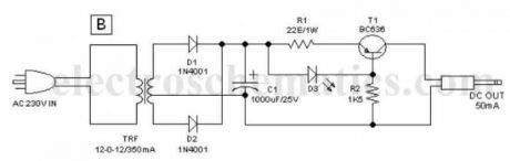
One very simple but reliable ac mains powered battery charger circuit for the handy pen torch is also included here. Basically the pen torch circuit is a constant current charger wired around Transistor T1 (BC636), powered by a 12v/350mA step down transformer and associated componentsD1, D2 and C1.
AC mains powered battery charger for the pen torch
Unregulated 12 volt dc available from the input power convereter circuit, comprising step down transformer(TRF), rectifier diodes (D1,D2) and filter capacitor (C1), is fed to T1 through a current limiting resistor R1. Grounded base PNP transistor T1 here works as a constant current generator. With 22 ohm resistor for R1, the charging current available at the output of the charger is near 50 mA.
Red LED (D3) provides a fixed voltage reference to the base of T1, with the help of resistor R2. (During charging process, Diode D1 in the main circuit prevent reverse current flow from the battery pack when charging input supply is absent.) After construction of the pen torch circuit, fit the assembled unit inside a small plastic enclosure for safety and convenience.?
2 Responses to “Handy Pen Torch circuit”
(View)
View full Circuit Diagram | Comments | Reading(2620)
| Pages:4/126 1234567891011121314151617181920Under 20 |
Circuit Categories
power supply circuit
Amplifier Circuit
Basic Circuit
LED and Light Circuit
Sensor Circuit
Signal Processing
Electrical Equipment Circuit
Control Circuit
Remote Control Circuit
A/D-D/A Converter Circuit
Audio Circuit
Measuring and Test Circuit
Communication Circuit
Computer-Related Circuit
555 Circuit
Automotive Circuit
Repairing Circuit