
Basic Circuit
Index 25
Relay Driver Output Schematic 2
Published:2013/6/25 22:32:00 Author:muriel | Keyword: Relay Driver Output Schematic
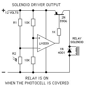
View full Circuit Diagram | Comments | Reading(1069)
Photocell Circuits Schematic
Published:2013/6/25 22:31:00 Author:muriel | Keyword: Photocell Circuits Schematic
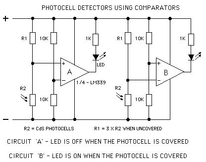
View full Circuit Diagram | Comments | Reading(1309)
Oscillator Made From A Comparator
Published:2013/6/25 22:29:00 Author:muriel | Keyword: Oscillator , Comparator
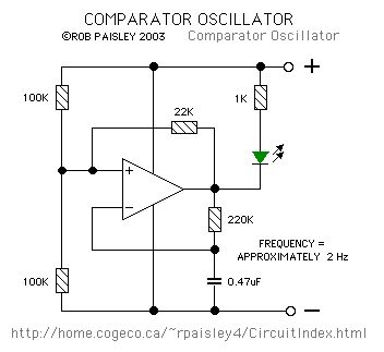
View full Circuit Diagram | Comments | Reading(1025)
Window Comparator
Published:2013/6/25 22:26:00 Author:muriel | Keyword: Window Comparator
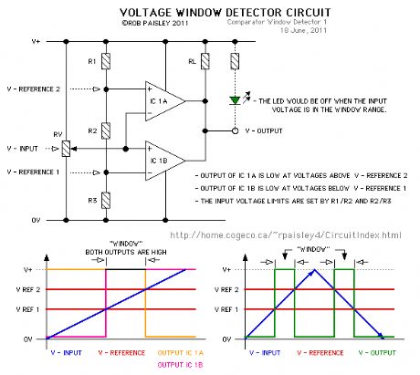
View full Circuit Diagram | Comments | Reading(5558)
Adding Hysteresis To The plus A Comparator
Published:2013/6/25 22:25:00 Author:muriel | Keyword: Adding Hysteresis , Comparator
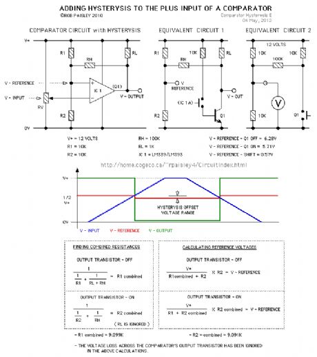
View full Circuit Diagram | Comments | Reading(825)
effect of input voltage offset on the output voltage
Published:2013/6/25 22:24:00 Author:muriel | Keyword: effect , input voltage , output voltage
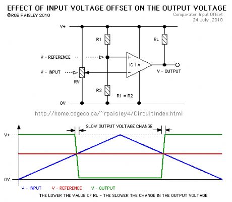
Voltage comparators are not perfect devices and their performance may suffer from the effects of a parameter known as the Input Offset Voltage. The Input Offset Voltage for many comparators is only a few millivolts and in most circuits can be ignored.
Problems related to the Input voltage normally occur when the Input voltage changes very slowly.
The net result of the Input Offset Voltage is that the output transistor does not fully turn on or off when the input voltage is close to the reference voltage.
The following diagram attempts to illustrate the effect of the input offset voltage with a slowly changing input voltage. This effect increases as the output transistor current increases so keeping the value of RL high will help reduce the problem. (View)
View full Circuit Diagram | Comments | Reading(1665)
comparator-input vs output rules
Published:2013/6/25 22:22:00 Author:muriel | Keyword: comparator-input vs output rules
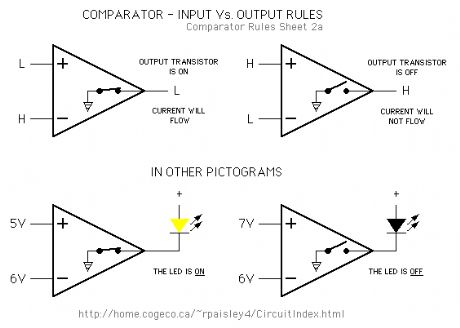
View full Circuit Diagram | Comments | Reading(1116)
basic operation of voltage compatators
Published:2013/6/25 22:20:00 Author:muriel | Keyword: basic operation , voltage compatators
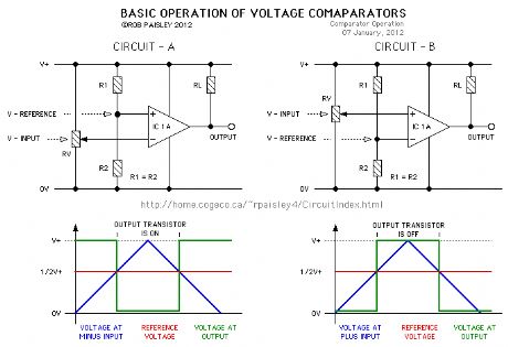
The following drawing show the two simplest configurations for voltage comparators. The diagrams below the circuits give the output results in a graphical form.For these circuits the REFERENCE voltage is fixed at one-half of the supply voltage while the INPUT voltage is variable from zero to the supply voltage.
In theory the REFERENCE and INPUT voltages can be anywhere between zero and the supply voltage but there are practical limitations on the actual range depending on the particular device used.
(View)
View full Circuit Diagram | Comments | Reading(939)
Dual Supply Comparator Equivalent circuit
Published:2013/6/25 22:19:00 Author:muriel | Keyword: Dual Supply , Comparator, Equivalent circuit
View full Circuit Diagram | Comments | Reading(814)
Comparator Equivalent Circuits For Single Power Supplies
Published:2013/6/25 22:15:00 Author:muriel | Keyword: Comparator Equivalent Circuits, Single Power Supplies
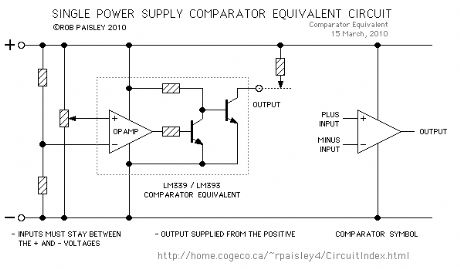
View full Circuit Diagram | Comments | Reading(1003)
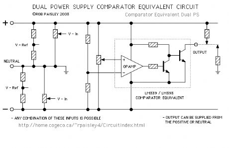
Dual Supply Comparator Equivalent
Published:2013/6/25 22:11:00 Author:muriel | Keyword: Dual Supply, Comparator Equivalent

View full Circuit Diagram | Comments | Reading(908)
5 Times Around Schematic
Published:2013/6/25 22:10:00 Author:muriel | Keyword: 5 Times Around Schematic
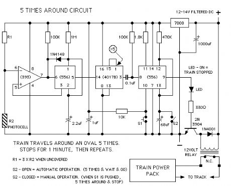
The 5 Times Around circuit was designed to automatically let an N Scale locomotive and car travel around a loop 5 times and stop for approximately a minute and then repeat the cycle. The loop of track was set up as an amusement park type of ride in the trolley section of The London Model Railroad Group's, 'O' scale layout. The club is located at London, Ontario, Canada. (View)
View full Circuit Diagram | Comments | Reading(884)
Multiple Solid State Relays
Published:2013/6/25 22:09:00 Author:muriel | Keyword: Multiple Solid State Relays
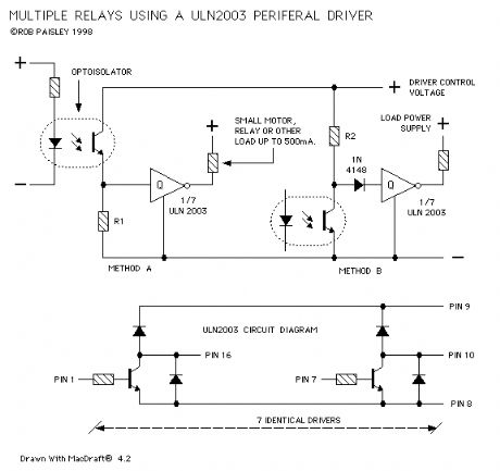
The next diagram shows an inexpensive method of building multiple medium current relays.
The circuit uses a ULN2003 - High voltage/High Current Peripheral Driver IC. This device can handle loads of 500 milliamps.
The IC is designed to have TTL and CMOS inputs of between 5 and 15 volts can be controlled by any clean input voltage.Two methods of controlling the ULN2003 are shown on the diagram. Method A is preferable and resistor R1 should be sized to pass about 1 milliamp.
Method B is OK but requires an extra diode to compensate for the voltage drop across the optoisolator transistor when it is conducting. If this diode was not used the transistor in the ULN2003 would not be able to turn off fully. Resistor R2 would also be sized to pass about 1 milliamp and the voltage drop across the drivers internal resistor will have to be taken into account.
As the peripheral drivers in the ULN2003 require only a small control current optoisolators with non darlington transistor outputs such as the 4N35 can be used.
There are other devices that are similar to the ULN2003, such as the ULN2803, which has eight drivers in an eighteen pin package. Other devices have higher or lower ratings and/or lack the protection diodes built into the ULN2003 package. (View)
View full Circuit Diagram | Comments | Reading(950)
Three Terminal Regulator Type Throttle
Published:2013/6/25 22:08:00 Author:muriel | Keyword: Three Terminal , Regulator Type, Throttle
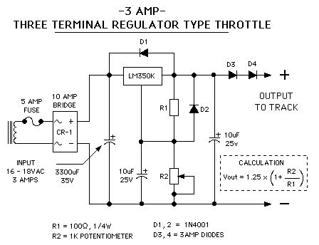
TTR Type Throttle Schematic
The schematic above is of a Three Terminal Regulator (TTR) design based on the LM350K adjustable voltage regulator which has a 3 Amp current rating as opposed to the LM317K with a 1.5 Amp rating. The LM 350 is internally protected from current and thermal overload and can be thought of as a high current version of the LM 317.
With the component values shown the circuit is designed to have and output voltage range of approximately 1.25 to 13.5 Volts when measured at the output of the regulator. The calculation on the drawing is used to determine the output voltage for given values of R1 and R2.
Because these regulators have a minimum output voltage of 1.25 Volts diodes D3 and D4 will provide a voltage drop of approximately 1.4 Volts so that zero output to the track can be obtained. These diodes need to have at least a 3 amp rating
The diodes D1 and D2 added to the circuit will prevent damage to the regulator during certain adverse conditions such as the output voltage being higher than the input voltage to the regulator. This can happen if this type of circuit is used as a variable power supply for an electronics test bench and without the added protection of D3 and D4.
A substantial heat sink will be needed for the TTR as quite a bit of heat will be generated when drawing high current with low output voltages. For this reason this circuit is not recommended for use in hand held throttles.
If the less expensive LM 317 regulator is used this circuit makes an excellent test bench power supply just leave out D3 and 4 and add a voltmeter. (View)
View full Circuit Diagram | Comments | Reading(1378)
DC Throttle Circuits 2
Published:2013/6/25 22:07:00 Author:muriel | Keyword: DC Throttle Circuits
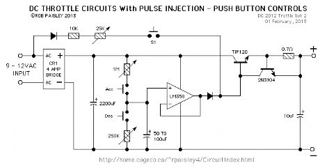
View full Circuit Diagram | Comments | Reading(1309)
DC Throttle Circuits
Published:2013/6/25 22:07:00 Author:muriel | Keyword: DC Throttle Circuits
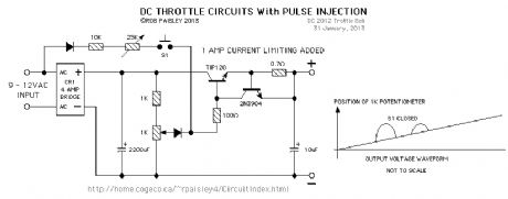
View full Circuit Diagram | Comments | Reading(908)
basic throttle 2
Published:2013/6/25 22:06:00 Author:muriel | Keyword: basic throttle
View full Circuit Diagram | Comments | Reading(751)
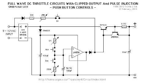
Fullwave DC Throttle Circuits With Clipped Outputs And Injected Pulses
Published:2013/6/25 22:06:00 Author:muriel | Keyword: Fullwave DC Throttle Circuits , Clipped Outputs , Injected Pulses
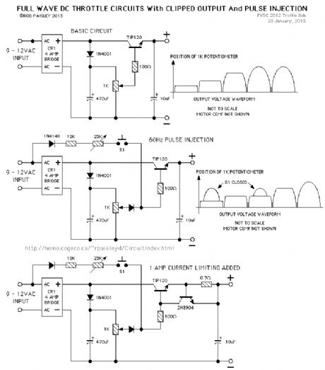
The following circuits are variations of a full wave DC throttles. The output voltage is clipped at a voltage level determined the 1K potentiometer so that the waveform is flat for most of the cycle. These throttles have good slow speed operation for typical DC motors.
A varialable level, 60Hz pulse injection scheme is also included, this could be used to boost the output voltage in difficult areas of track, used to make the locomotive creep or perhaps as a kicker when shunting.
(View)
View full Circuit Diagram | Comments | Reading(863)
Full Featured Toy Throttle
Published:2013/6/25 22:05:00 Author:muriel | Keyword: Full Featured Toy Throttle
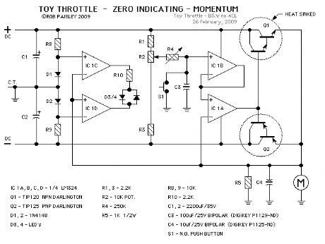
The next schematic shows a full featured Toy Throttle Upgrade. This version has Zero Indication, and Momentum.
The transformer and bridge rectifier have been omitted to make the drawing smaller.All of the features in this circuit can be found in conventional throttle designs. The only difference here is the PLUS or MINUS output voltage capability. (View)
View full Circuit Diagram | Comments | Reading(632)
Zero Indicator Option
Published:2013/6/25 22:04:00 Author:muriel | Keyword: Zero Indicator Option
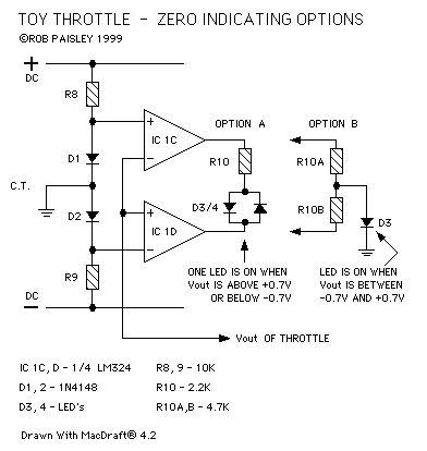
View full Circuit Diagram | Comments | Reading(625)
| Pages:25/471 At 202122232425262728293031323334353637383940Under 20 |
Circuit Categories
power supply circuit
Amplifier Circuit
Basic Circuit
LED and Light Circuit
Sensor Circuit
Signal Processing
Electrical Equipment Circuit
Control Circuit
Remote Control Circuit
A/D-D/A Converter Circuit
Audio Circuit
Measuring and Test Circuit
Communication Circuit
Computer-Related Circuit
555 Circuit
Automotive Circuit
Repairing Circuit