
Motor Control
Index 4
FM/FSK 433MHz Emitter Circuit Diagram
Published:2011/6/19 7:03:00 Author:Vicky | Keyword: FM/FSK 433MHz Emitter Circuit
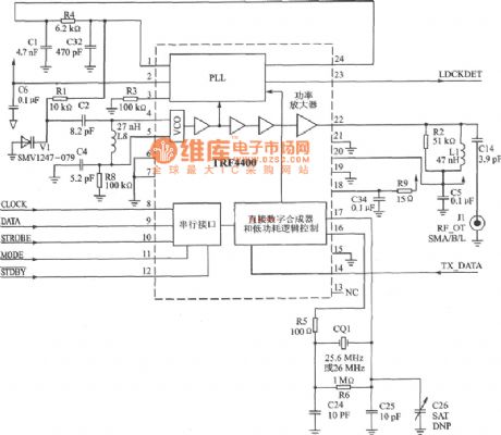
Circuit of TRF4400 application in 433 MHz IS
TRF4400 is an multi-chanell low-cost emitter which can provide full functions. The can meet the requirement of 433MHz frequency band linear (FM) or application of digital(FSK) emitter.
Main technical features are listed as follows:
·Work frequency: 420~450 MHz;
·FM/FSK modulation mode;
·Small demand of exterior fittings;
·Work voltage: 2.2~3.6 V;
·Typical emitting power: 7 dBm;
·Maximum work current of emitter: 75 mA,low-power dissipation mode: 0.5μA;
·Flexible serial interface to be connected to T1 MSP430 microcontroller.
(View)
View full Circuit Diagram | Comments | Reading(1196)
MHz-KH Series Encoding Emitter Module Circuit Diagram
Published:2011/6/26 8:03:00 Author:Vicky | Keyword: MHz-KH Series Encoding Emitter Module
\TXE-433/418/315 MHz—KH series encoding emitter module
TXE-433/418/315 MHz—KH series encoding emitter module , when used together with KH decoding receptor module, can form a highly-reliable wireless link, which send 1 to 8 parallel input states; the address coding is 310 groups; the transmitting distance is over 91.5 m(300 ft). The correspondent receptors are RXD-315-KH(315 MHz)、RXD-418-KH(418 MHz)和RXD-433-KH(433 MHz).
KH series radio frequency encoding emitter is available in remote control system , keyless entering system, garage gate control, lightening control system etc.
Main technical features are listed below:
·No need of other exterior radio frequency component except antenna;
·Maximum output power: +4 dBm;
·Emitting data length: 26 bytes×3
·Work voltage: 2.7~5.2 V;
·Work current: l.5 mA,sleeping mode current: lμA。
(View)
View full Circuit Diagram | Comments | Reading(651)
MHz-LC Series Emitter Module Circuit Diagram
Published:2011/6/19 4:21:00 Author:Vicky | Keyword: MHz-LC Series Emitter Module
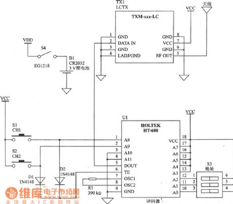
TXM-433/418/315 MHz-LC series module is a low-cost emitter module. It is used with LC series receptor and can transmit analog and digital signal for over 91.5 min (300 ft). LC series requires no tuning device or exterior RF components (except antenna). It is available to be applied in fields such as remote control, remote monitoring, industry process monitoring, periodic data transfer, illuminator control, safe/fire alarm, keyless typing system, medical monitoring/calling system and wireless data transfer etc.
Main technical features are listed as follows:
·Work frequency: 433/418/315 MHz;
·Direct analog or digital input;
·Data transfer rate: greater than 5 Kb/s;
·Voltage of power supply: 2.7~5.2 V;
·Maximum work current: 6MA, sleep mode current: l.5 μA;
·Output power: -4~4 dBm;
·Direct series interface. (View)
View full Circuit Diagram | Comments | Reading(1197)
MHz-RM Series FM/FSK Emitter Module Circuit Diagram
Published:2011/6/19 4:23:00 Author:Vicky | Keyword: MHz-RM Series FM/FSK Emitter Module
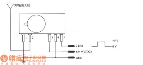
TXM-433/418 MHz-RM series is emitter moduel based on SAW. It is used with RM series receptor and can transmit analog and digital signal for over 152.5m (500 ft). RM series module requires no tuning, regulating or exterior RF component (except antenna). It is available to be applied in fields such as remote monitoring, industry process monitoring, periodic data transfer, illuminator control, safe/fire alarm and remote control etc.
Main technical features are listed as follows:
·Direct analog or digital input;
·Data rate: greater than 10 Kb/s;
·Voltage of power supply: 5.9~9 V;
· Work current: 6 mA.
(View)
View full Circuit Diagram | Comments | Reading(968)
Electronic timer switch circuit
Published:2011/6/27 2:52:00 Author:Fiona | Keyword: Electronic timer, switch
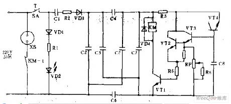
Close the power switch sA,the LED vD2 indicates the work,reduces the voltage by limiting resistor R2 and capacitance c1,rectifys by diode VD3,then filters by balanced symmetrical capacitance c2—c7 and obtains the 6v DC voltage in C7 ends.Because the backward resistance of the emitter junction is large and the input resisters of transistors VTl,VT2,VT3 are connected,The resistance is also very large,so this circuit can increase regular time.When turn on the power,the capacitor c8's voltage is Uc8 = oV, vTl, vT2, VT3 are cut off.vT4 provides the constant charging electric current to C8to make the Uc8 hasten linear growth.
(View)
View full Circuit Diagram | Comments | Reading(1081)
The door control,light-dependent control switch circuit
Published:2011/6/27 23:45:00 Author:Fiona | Keyword: The door control, light-dependent control
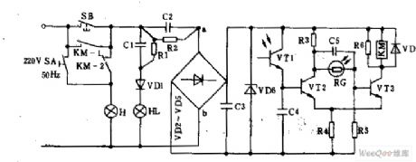
When opens the door,the contact of the key switch SB is closed.The city power reduces voltage by the capacitor C1,rectifys by the diode VDl,indicator light LED is lit.At the same time,the city power reduces voltage by c2,then outputs 12v dc voltage by c3 after filtering. During the day,the resistance of the phototransistor VTl becomes smaller by the light, when it reaches a - threshold, vT2 conducts, the collector of vT2 is low, although thelight dependent resistor RG receives the light but it can not make VT3 conduct.The relay KM is no electricity,the contact KM-1, KM-2 are off,floodlight H is not bright.
(View)
View full Circuit Diagram | Comments | Reading(693)
Optical remote control power switch circuit
Published:2011/6/28 0:12:00 Author:Fiona | Keyword: Optical remote control, power switch
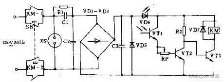
It is a light-controlled power remote control equipment,it can be used for the light of the torch triggering.The circuit consists of two parts:one is the light control circuit;the other one is controlled circuit.The light-controlled part consists of the photoelectric transistor VT1,transistor potentiometer RP and phase transistor VT2.The controlled part consists of the transistor VT3 and the relay KM.When the key switch SB is pressed,the both ends of the voltage-regulator diode vD5 obtains the l 2V DC voltage.The light-emitting diode VD6 displays work.Resistor Rl provides bleeder current loop to the capacitor C1.vD7 is the protection diode.
(View)
View full Circuit Diagram | Comments | Reading(1150)
FSK/ASK 433MHz Emitter Circuit Diagram
Published:2011/6/19 5:15:00 Author:Vicky | Keyword: FSK/ASK 433MHz Emitter
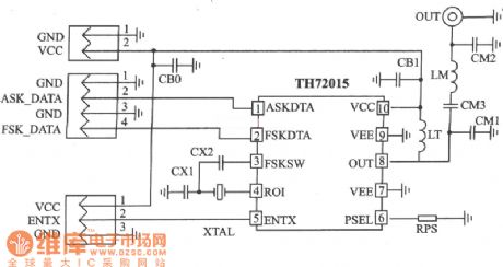
TH72015 applied circuit
TH72015 is a FSK/ASK emitter specially designed for application for European 433 MHz ISM frequency range, which reaches EN 300 220 wireless communication standard. It is available for application in keyless entering system, remote control/remote-measuring system , data communication system and security system etc.
Main technical features are as follows:
·Work frequency: 380~450 MHz;
·Singal-ended RF output;
·FSK modulation rate: DC~40 Kb/s;
·ASK modulation rate up to 40 Kb/s;
·Voltage of power supply: l.9~5.5 V;
·Work current: 3.5~10.7 mA, stand-by current: 0.1μA;
·Output power: -12~+8.5 dBm.
(View)
View full Circuit Diagram | Comments | Reading(1440)
ASK 433MHz Emitter Circuit Diagram
Published:2011/6/19 5:17:00 Author:Vicky | Keyword: ASK 433MHz Emitter
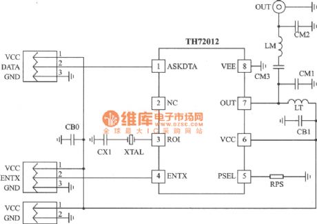
TH72012 applied circuit
TH72012 is monolithic emitter chip which reaches standard of EN 300 220 and the analogs. It is available for keyless entering system, remote control/ remote measuring system, data communication system and security system etc.
Main technical features are as follows;:
·Completely integrated and stable PLL;
·Work frequency: 380~450 MHz;
·Single-ended RF output;
·ASK modulation mode;
·ASK modulation rate up to 40 Kb/s;
·Voltage of power supply: l.9~5.5 V;
·Work current: 3.5~10.7 mA, stand-by current: 0.1μA;
·Output power: -12~+8.5 dBm. (View)
View full Circuit Diagram | Comments | Reading(855)
FSK 433MHz Emitter Circuit Diagram
Published:2011/6/19 7:23:00 Author:Vicky | Keyword: FSK 433MHz Emitter
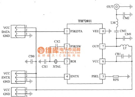
TH72011 applied circuit
TH71072 is a monolithic emitter chip which reaches standards of EN 300 220 and the analogs. It is available for keyless entering system, remote control/remote measuring system, data communication sysytem and security sysetem etc.
Main technical features are as follows:
·Completely integrated and stable PLL;
·Work frequency:380~450 MHz;
·Single-ended RF output;
·FSK modulation mode;
·FSK carrying out modulation driven by crystal oscillator, FSK modulation rate: DC~40 Kb/s;
·Voltage of power supply: 1.9~5.5 V;
·Work current: 3.5~10.7 mA,stand-by current 0.1μA;
·Output power: -l2~+8.5 dBm. (View)
View full Circuit Diagram | Comments | Reading(1132)
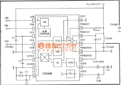
ASK 440~310MHz Emitter Circuit Diagram
Published:2011/6/19 7:26:00 Author:Vicky | Keyword: ASK 440~310MHz Emitter
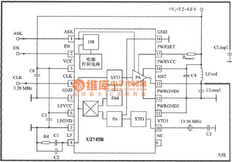
U2745B is a PPL emitter chips specially designed for low-cost data communication, which is available for application in wireless temperature measuring, keyless keyboard, gate lock, light, fan, air-conditioner, shutter control and other consumer products.
Main technical features are as follows:
·Emitter frequency: 310~440 MHz;
·ASK modulation mode;
·Voltge of power supply: 2.2~4 V;
·Maximum output power: 5 dBm(Vs=3 V,f=433.92 MHz,RPWRSET=l.2 kΩ);
·Maximum power dissipation: 250 mW;
·Maximum work current: l2.5 mA,maximum current udner low-power dissipation mode 10μA;
·Maximum data transfer rate: 20 Kb/s;
·Microprocessor clock signal ,which can be compatible with microcontroller such as M44C090 and M44C890;
·ESD protection (excluding pins XT02 and XT01)as requested by MIL-STD.883(4KV HBM);
·Work temperature: -20~+70℃. (View)
View full Circuit Diagram | Comments | Reading(1395)
ASK/FM 433/315 MHz Emitter Circuit Diagram
Published:2011/6/19 7:29:00 Author:Vicky | Keyword: ASK/FM 433/315 MHz Emitter
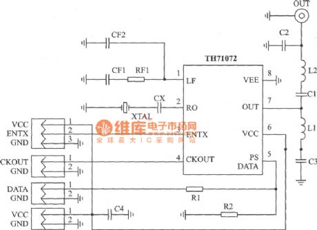
TH71071 applied circuit
TH71071 is a monolithic emitter chip which reaches standards of EN 300 220 and the analogs. It is available for keyless entering system, remote control/remote measuring system, data communication sysytem and security sysetem etc.
Main technical features are as follows:
·Work frequency range: 310~440 MHz;
·ASK/FM modulation mode;
·ASK is conducted by interior power amplifier/gained by closing keying
·FM which makes use of externally-linked variode
·Voltage of power supply: 2.2~5.5 V;
·Work current: 4.8~11.5 mA, maximum stand-by current: 0.1μA;
·Output power: -12~+2 dBm. (View)
View full Circuit Diagram | Comments | Reading(912)
FM Emitter Module Circuit Diagram
Published:2011/6/19 7:59:00 Author:Vicky | Keyword: FM Emitter Module
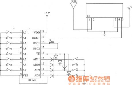
T5 is a micro UHF emitter module and is used with receptor module R5. It is suitable for application in one point to one point or multipoint connection, such as vehicle warning system, remote control of warehouse gate and house & commerce security system.
Main technical features are as follows:
·Work frequency: 433.92 MHz;
·Data transfer rate up to l28 Kb/s;
·Emitting distance up to 300 m;
·Voltage of power supply: 4.5~5.5 V;
·Maximum work current: l2 mA;
·Maximum RF power: +12 dBm. (View)
View full Circuit Diagram | Comments | Reading(733)
Radio Frequency Modulator Circuit Diagram
Published:2011/6/19 9:11:00 Author:Vicky | Keyword: Radio Frequency Modulator
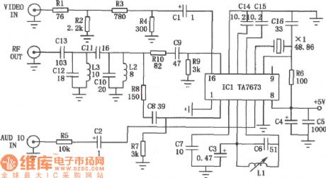
The above picture is the detailed circuit of radio frequency modulator. IC1 is integrated circuit TA7673 especially for modulator, the pins 10 & 11 of which produce picture carrier signal by externally connection to crystal oscillator, and pins 4 & 5 of which produce 6.5MHz secondary audio signal. Audio signal is input via pin 6 of ICl, and video signal is input via pin 16 of ICl. When crystal oscillators of different work frequency are connected to part between pin 10 and pin 11 , the circuit can then give out picture carrier signal from channel 1 to 5 in pin 2 and pin 15. The circuit doesn’t need debugging after finishing assembly, but the whole circuit uses small metal-box as shield. (View)
View full Circuit Diagram | Comments | Reading(1719)
Motor Operation Control Circuit of LT1014
Published:2011/6/25 22:44:00 Author:Michel | Keyword: Motor, Operation , Control Circuit
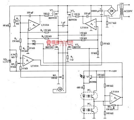
The aboved picture is motor operation control circuit compsoed of LT0140 etc.Motor speed voltage is set by middle tap of potentiometer RP1.In order to make the motor speed stable, RP3 adjusts the positive feedback voltgae from current detection resistance R1 is inversely proportional to the current and A1 adds the feedback voltage and speed setting voltage together.The best RP3 adjustment can completely offset the motor parasitic resistance, so that motor torque-speed characteristics are hard.Motor speed control performance does not depend on mechanical loading, but driving circuit voltage. (View)
View full Circuit Diagram | Comments | Reading(1091)
Capacitive dimmer switch circuit
Published:2011/6/25 9:28:00 Author:John | Keyword: switch
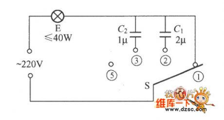
Capacitive dimmer switch circuit is as shown. It uses the principle of capacitance of capacitors for AC. When the S is at the shown position, bulb E normally lights with the maximum brightness. When it is dialed to position ②, light intensity of E decreases because of the insert of 2μF capacitor C1 in series. When it is allocated to the position ③, the brightness is reduced with a block because of increasing capacitance cause by C2 <C1. And when it is allocated to the position ④, the light E is off. C1 and C2 should use non-polar oil paper capacitor which can endure more than 400V voltage. And S is the 1 × 4 single-pole four-throw switch.
(View)
View full Circuit Diagram | Comments | Reading(924)
OOK 315MHz Emitter Module Circuit Diagram
Published:2011/6/19 3:54:00 Author:Vicky | Keyword: OOK 315MHz Emitter Module
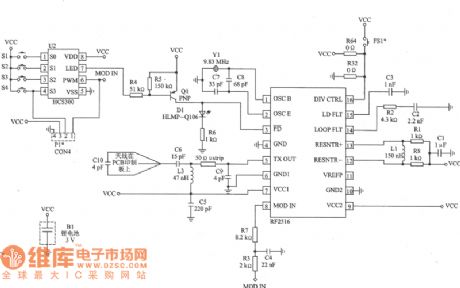
DKl000T is an emitter module composed by RF2516 and roll-code encoding device. Correspondingreceptor module is DKl000R. DKl000T is suitable to be applied in keyless-entering system, wireless safe system, remote monitoring and remote control.
Main technical features are listed as follows:
·Operating frequency: 315MHz;
·Modulation mode of 00K;
·Roll-code encoding;
·LED indicator;
·Output power: 70 dBμV/m 5;
·Voltage of power supply: 2~3 V ;
·Dissipation of current: 4~9 mA;
· Printing the antenna in the printing board.
Applied circuit of DKl000T module 315Hhz
(View)
View full Circuit Diagram | Comments | Reading(1349)
ASK/FSK 450~300MHz Emitter Circuit Diagram
Published:2011/6/18 10:42:00 Author:Vicky | Keyword: ASK/FSK 450~300MHz
U27418 is a PLL emitter chip specially designed for meeting the low cost of data communication. The corresponding receiver chip is U3741.
Main technical features are listed as follows:
·Emitting frequency: 300~450 MHz;
·Modulation mode of ASK/FSK;
·Maximum transmission rate: 0 Kb/s;
·Voltage of power supply: 2.O~5.5 V;
·Maximum output power: 5 dBm(Vs=3 V,f=433.92 MHZ 9RPWRSET=1.2 kΩ);
·Maximum dissipation of power: 250 mW ;
·Maximum work current : l2.5 mA, maximum current of low-power mode: 0.35μA ;
·Microprocessor clock signal ,which can be compatible with microcontroller such as M44C090 and M44C890;
·ESD protection (excluding pins XT02 and XT01)as requested by MIL-STD.883(4KV HBM);
·Work temperature: -20~+70℃.
Applied circuit of U2741
(View)
View full Circuit Diagram | Comments | Reading(1747)
Stepper Motor Typical Application Circuit
Published:2011/5/19 6:15:00 Author:Robert | Keyword: Stepper Motor, Typical Application
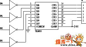
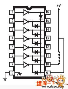
The ULN2003A type high-voltage large-current darlington transistors array circuit's typical application circuit diagram is shown in the picture below. The clamping diode is used for protecting the integrated circuit from been punctured by the EMF when the coil is connected or disconnected. It can be seen that this circuit's application is very simple.
The stepper motor typical application circuit is shown below.
(View)
View full Circuit Diagram | Comments | Reading(1004)
Adjustable timing hige automatic switch circuit
Published:2011/6/8 6:46:00 Author:Fiona | Keyword: Adjustable timing hige automatic switch
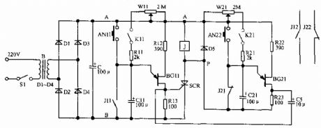
Button switch AN11, AN2 is manual on and off. K11 and K22 is a separate automatic delay on and off. When connecting the power, the circuit charges to the C11 through the W11 and R11, when the voltage of the capacitor is above the peak of BG11, BG11 conducts to trigger the SCR conducts, the relay J is energized pick, J12 and J22 moves to control appliances. J11 closes to discharge the charge on the C11, BG11 closes. During the regular open, when SCR guides energy,point P is equivalent to grounding, often close point J12 is off, by the current charges to C21 through W21 and R21, when the voltage of C21 ends is higher than the peak of the BG21, BG21 conducts, the output signal makes SCR off by C5, the relay disconnects after losing the power, circuit resets.
(View)
View full Circuit Diagram | Comments | Reading(656)
| Pages:4/6 123456 |
Circuit Categories
power supply circuit
Amplifier Circuit
Basic Circuit
LED and Light Circuit
Sensor Circuit
Signal Processing
Electrical Equipment Circuit
Control Circuit
Remote Control Circuit
A/D-D/A Converter Circuit
Audio Circuit
Measuring and Test Circuit
Communication Circuit
Computer-Related Circuit
555 Circuit
Automotive Circuit
Repairing Circuit