
Motor Control
Index 3
Nine key coded lock circuit composed of CD4017
Published:2011/7/20 20:21:00 Author:Fiona | Keyword: Nine key, coded lock
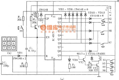
View full Circuit Diagram | Comments | Reading(990)
Safe and reliable coded lock (CD4017) circuit
Published:2011/7/20 20:23:00 Author:Fiona | Keyword: Safe and reliable, coded lock
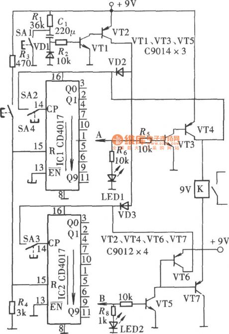
View full Circuit Diagram | Comments | Reading(1026)
Super coded lock circuit composed of CD4017
Published:2011/7/20 20:24:00 Author:Fiona | Keyword: Super coded lock
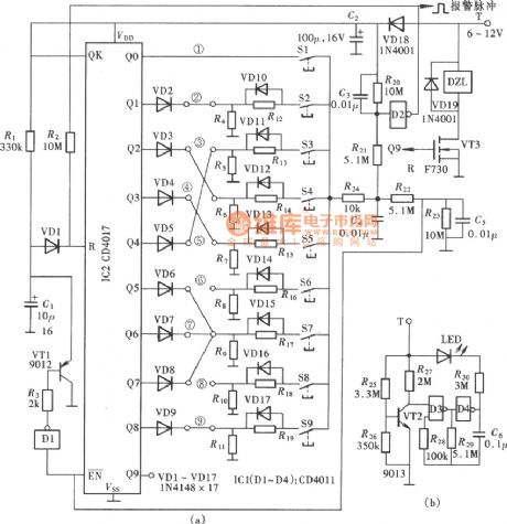
View full Circuit Diagram | Comments | Reading(734)
Three-phase and Six-step Motor Control Circuit of MC33035
Published:2011/7/13 7:06:00 Author:Michel | Keyword: Three-phase, Six-step, Motor Control Circuit
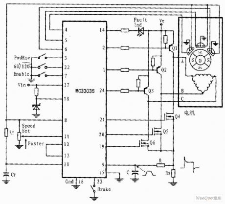
The shown three-phase application circuit owns motor controller circuit connection diagram which is driven by full wave six-step.The power switch triode is Darlington PNP type and the lower power switch triode is N groove power MOSFET. Each device contains a parasitic catching diode thus it can make stator inductance energy return power supply.The output can drive triangle or star connecting stators.The neutral grounded Y connection can be driven if the split power is used.
In any given rotor position,the circuit shown in picture 3 only has an effective top and bottom power switch(They belong to different totem columns). (View)
View full Circuit Diagram | Comments | Reading(7079)
Video switch using MC1545 circuit
Published:2011/7/12 10:02:00 Author:John | Keyword: Video switch

Video switch using MC1545 circuit is as shown. MC1545 is the gated broadband amplifier, which is used as a video switch. The input is with differential mode. The door switch is used to convert two amplifiers A and B. A is selected to high electricity level and B is for low one. The output is also with differential output terminals. Gate input signal refers to TTL level, whose gated conversion time can be 20ns. When the gate signal is at high level, the video input signal is taken as an output signal. When the gate signal is at low level, the amplifier A is at the off state.
(View)
View full Circuit Diagram | Comments | Reading(599)
Video switch circuit
Published:2011/7/12 10:06:00 Author:John | Keyword: Video switch
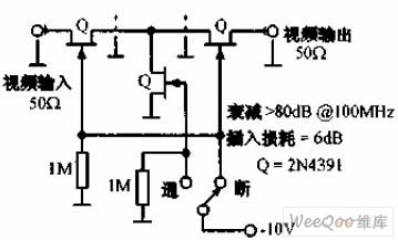
Video switch circuit is as shown. 2N4391 FET provides the circuit with only 30Ω induction -resistance and less than 0.2pF pinch-off is capacitance. This performance can be comparable with that of the ideal high-frequency switch. The attenuation for 100MHz circuit is more than 80dB and the insertion loss is about 6dB.
(View)
View full Circuit Diagram | Comments | Reading(712)
DPDT FET switch circuit
Published:2011/7/12 10:13:00 Author:John | Keyword: DPDT FET switch, FET
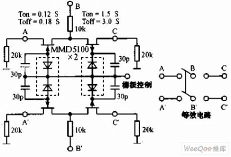
DPDT FET switch circuit is as shown. When the FET is inducted, the resistance of the drain channel can be up to thousands of MΩ. Therefore, FET can constitute an ideal low-frequency switch. Capacitance of ends of the FET is not good to do isolation for high-frequency signals. Thus, response time can be increased and maximum operating frequency can be limited.
(View)
View full Circuit Diagram | Comments | Reading(1253)
Brushless DC Motor Driving Circuit
Published:2011/7/17 7:12:00 Author:Robert | Keyword: Brushless, DC, Motor, Driving
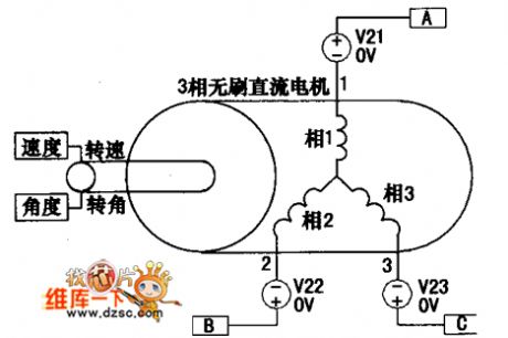
The brushless DC motor driving circuit is shown in the picture. (View)
View full Circuit Diagram | Comments | Reading(1134)
Wire connection incandescent lamp life extension switch circuit
Published:2011/7/4 0:46:00 Author:John | Keyword: switch, incandescent lamp
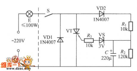
A wire connection incandescent lamp's life extension switch is shown. As its warm-up time is long, the service life of the bulb E is long. When the switch S is closed, 220V AC only has the negative half-cycle and powers bulb E through the VD1 and S. At this time, it is under the semi-pressure warm-up state. AC’s positive half-cycle charges the capacitor C through the VD2 and R1 and R2 divider until the voltage across C rises to more than 3V. Then the regulator thyristor VS is breakdown to conduct VT. Therefore, the bulb E is under total pressure to light.
(View)
View full Circuit Diagram | Comments | Reading(964)
Timed trigger switch circuit
Published:2011/7/1 5:51:00 Author:Fiona | Keyword: timed, trigger switch
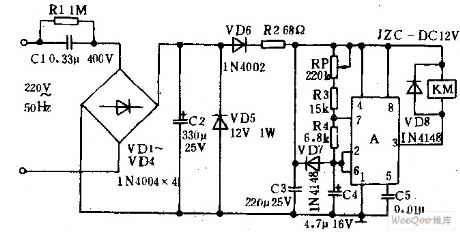
The AC power source reduces the voltage by the capacitance C1,bridge rectifies by diode vDl—vD4,filters by the capacitor C2 and obtains the 12V DC voltage in both ends of the diode VD5.After rectifying and current-limiting by the diode vD6 and resistor R2,the supply voltage charges the capacitor c4 by potentiometer RP, and resistors R3, R4.When the voltage of the A's ② ⑥ pins is greater than 2 / 3 supply voltage because of c4 both ends voltage being charged to time base integrated circuit, A is in reset state, its ③ pin is low,the relay KM is closed to make the moving contacts are launched to control the trigger circuit or lanterns.
(View)
View full Circuit Diagram | Comments | Reading(721)
The switching solenoid driver circuit
Published:2011/7/8 3:18:00 Author:Fiona | Keyword: switching solenoid

The picture shows the switching solenoid driver circuit,the device U8 is 74123 chip, the device 02,03 are solid-state relays,coil PUSH is the switching inhaled coil,HOLD's ability is to maintain the coil,the power supply VDD is 24V.When the switching mechanism converts to dual fuel conversion mechanism working condition,Y1 input from 74123's B pin jumps from low to high.This change will make 74123's the output end Q input a transient high current pulse,the maintain time is ΔT.After the inverter 7404,the potential UA of A-point will appear the same width of pulse low level,the input of solid-state relay 02 has ΔT time current passed,when the output of the solid-state relay 02 has ΔT time conduction.
(View)
View full Circuit Diagram | Comments | Reading(1871)
ASK/FM 433/315MHz Emitter Circuit Diagram
Published:2011/7/10 6:05:00 Author:Vicky | Keyword: ASK/FM 433/315MHz Emitter
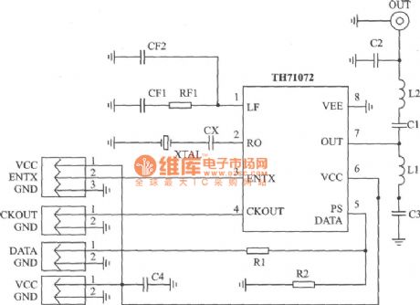
TH71072 applied circuit
TH71072 is a monolithic emitter chip which reaches standards of EN 300 220 and the analogs. It is available for keyless entering system, remote control/remote measuring system, data communication sysytem and security sysetem etc.
Main technical features are as follows:
·Work frequency range: 310~440 MHz;
·ASK modulation mode;
·ASK is conducted by interior power amplifier/gained by closing keying
·FM which makes use ofvariode which is connected externally
·Voltage of power supply: 2.2~5.5 V;
·Work current: 4.8~11.5 mA;
·Output power: -151~-1 dBm. (View)
View full Circuit Diagram | Comments | Reading(888)
ASK 320~290MHz Emitter Circuit Diagram
Published:2011/7/7 8:26:00 Author:Vicky | Keyword: ASK 320~290MHz Emitter
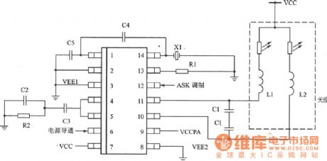
KESTX02 is a monolithic ASK emitter chip which meets therequirment of the basic power of FCC part l5 and harmonic suppression and is suitable for application of underpower wireless.
Main technical features are listed as follows:
·Operating frequency: 290~320 MHz;
·Complete integration of VC0, PLL and power amplifier;
·Low dissipation of current and improve of battery usage duration;
·Voltage of power supply: 3.5~6.5 V;
·Regulation of output power;
·Maximum work current: l2 mA, low power mode current: 0.7μA;
·Cheap exterior fittings.
Applied circuit of KESTX02
(View)
View full Circuit Diagram | Comments | Reading(740)
Single metal chip touch switch circuit
Published:2011/7/9 1:57:00 Author:Fiona | Keyword: Single metal chip
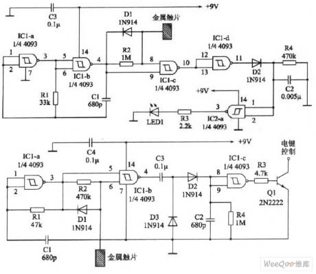
The circuit shown in the figure only uses a touch metal chip,the circuit uses two forty-two input terminals(internal has four identical, with two input terminals) schmitt trigger 4093(such as CD4093,TC4093 etc.).Usually the output terminal's 3 pin of IC2-a is low,light-emitting diode LED1 can not shine,when touching metal chip, the output terminal changes into high level to make the LED1 turn and light.
(View)
View full Circuit Diagram | Comments | Reading(2107)
Stepper Motor ULN2003 Internal Diagram And Equivalent Circuit
Published:2011/7/8 23:31:00 Author:Robert | Keyword: Stepper Motor, Internal, Diagram, Equivalent

In practice general driving channels is more than one. But using the discrete circuit shown in the picture will get large volume. So in many cases it always uses ready-made ICs for multi-channel driving. Commonly used small type stepper motor driving circuit can be ULN2003 or ULN2803. This book's auxiliary experiment board uses the ULN2003. ULN2003 is one of the high-voltage large-current darlinton transistor array series products. It features high current gain, high working voltage, wide temperature range, high loading capacity and so on. So it is adequate to many kinds of high-speed large-power driving systems. The ULN2003A is made up of 7 groups darlinton transistor arrays and corresponding resistances network and clamping diodes network. It has the load capacity of driving 7 groups at the same time. It is a single-chip bipolar large-power high-speed IC. The ULN2003 internal structure and its equivalent circuit is shown in the picture. (View)
View full Circuit Diagram | Comments | Reading(3055)
Switching power supply circuit with low-noise RCC mode
Published:2011/7/9 4:31:00 Author:chopper | Keyword: Switching, power supply, low-noise, RCC mode

Figure shows the grid drive circuit which uses the saturable reactor,switching power supply with low-noise RCC mode.Its output is 24V/4.5A, and it is as example of soft switching applications.
(View)
View full Circuit Diagram | Comments | Reading(3706)
Metal Proximity Switch
Published:2011/7/7 2:34:00 Author:Felicity | Keyword: Metal Proximity Switch
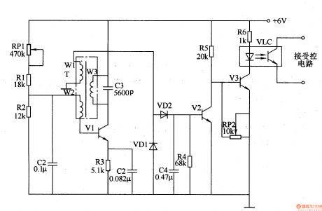
Work of the circuit The circuit consists of high-frequency oscillator circuit, voltage rectifier circuit, and electronic switching circuit. (It is showed in picture 8-131.)High-frequency oscillator circuit consists of high frequency transformer T, potentiometer RPl, resistors Rl-R3, capacitor Cl-C3 and transistor Vl.Voltage rectifier circuit consists of diode VDl and VD2, capacitor C4 and resistor R4.Electronic switching circuit consists of transistor V2 and V3, potentiometer Rm, optocouplers VLC and resistors R5, R6. (View)
View full Circuit Diagram | Comments | Reading(939)
Using IRFP250 power tube H-bridge motor drive circuit
Published:2011/7/8 2:42:00 Author:Fiona | Keyword: power tube, H-bridge motor drive
The drive circuit of electromotor includes a FET bridge circuit, FET base drive circuit,current sensor of motor drive circuit and the relay. FET bridge circuit mainly consists of four high-power MOSFET power tubes,it requires that the power tubes have good switching characteristics,can withstand higher drive current and have a long life.According to motor power parameters and power tube limit parameters and the electrical characteristics,we use four the same N-channel IRFP250power tubes to form the H-bridge circuit.
(View)
View full Circuit Diagram | Comments | Reading(6903)
Motor Control Circuit of VFC320
Published:2011/6/26 5:04:00 Author:Michel | Keyword: Motor Control, Circuit
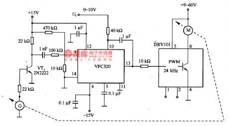
The aboved picture is the motor control circuit composed of VFC320.Tachogenerator G outputs AC current which is correspondent to motor speed.VTl circuit converts it into the narrow negative pulse and trigger frequency/voltage converter VFC320.There are operational amplifiers in VFC320 chip and they are used as the integratorof the speed control loop. When integrator receives the input control voltage of the corresponding average current of equal and opposite direction and the single trigger pulse current added to frequency/voltage converter feedback loop reaches balanced condition.DRVlO1 driver is used in motor and its maximum output current is 1.9 A and which is enough to drive the ordinary motor. (View)
View full Circuit Diagram | Comments | Reading(1387)
Voltage-Regulator Diode Performance Quick Test Circuit Diagram
Published:2011/6/26 6:12:00 Author:Vicky | Keyword: Voltage-Regulator Diode Performance Quick Test
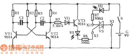
As shown in the picture, VT1 & VT2 etc constitute astable free-running multivibrator and the vibrator’s frequency is determined by C1, R2,R3, C2 etc. The cycle of the vibrator is about 4 seconds. VT2 gives out high level, the level then is transformed by VD, and VT3 is conducted, meanwhile the current is limited by luminous diode H1 and resistance R6, and finally it triggers bidirectional diode thyristor. A good thyristor is immediately conducted, and luminous diode H2 gives out light; when VT2 gives lout low level, VD, VT3, VS all end and H2 is lightless. If H1 and H2 shines synchronously , the thyristor is good; if H1 shines while H2 is extinct, then VS suffers internal short-circuit; if H2 remains luminous all the time, then VS suffers internal breakdown; if both H1 and H2 don’t shine, then VT1 and VT2 circuit don’t vibrate. (View)
View full Circuit Diagram | Comments | Reading(892)
| Pages:3/6 123456 |
Circuit Categories
power supply circuit
Amplifier Circuit
Basic Circuit
LED and Light Circuit
Sensor Circuit
Signal Processing
Electrical Equipment Circuit
Control Circuit
Remote Control Circuit
A/D-D/A Converter Circuit
Audio Circuit
Measuring and Test Circuit
Communication Circuit
Computer-Related Circuit
555 Circuit
Automotive Circuit
Repairing Circuit