
Signal Processing
Index 186
1500W square-wave inverter
Published:2011/4/26 3:43:00 Author:May | Keyword: 1500W, square-wave inverter
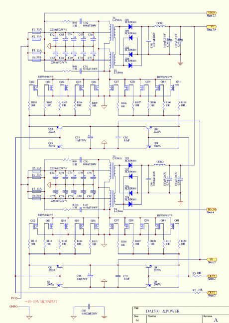
View full Circuit Diagram | Comments | Reading(1896)
Music control colored light circuit diagram
Published:2011/4/20 9:45:00 Author:Rebekka | Keyword: Music control colored light
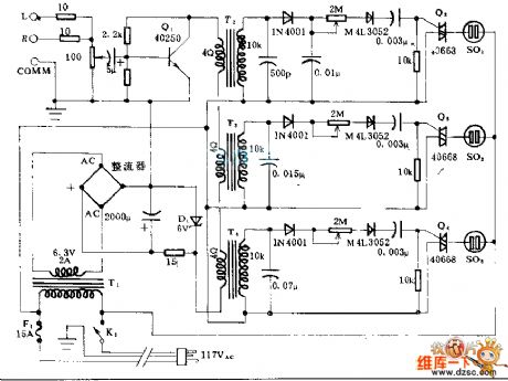
This circuit only use three channels for acousto-optic conversion, as the Yin additional stereo equipment. To remove the heavy DC load, the circuit use triac instead of an ordinary silicon. Capacitance Road and audio transformer T2 ~ T ¥ is parallel. They are transferred to high, medium and low frequency range. Triac TRIAC Q2 ~ Q1 turn on the colored bulbs inserting into the outlet SO.
(View)
View full Circuit Diagram | Comments | Reading(1662)
1024kHz and 4kHz square-wave output circuit
Published:2011/4/21 5:14:00 Author:Ecco | Keyword: 1024kHz , 4kHz , square wave, output
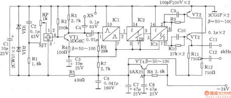
The circuit SJT is a 1024kHz warming crystal oscillator. Circuit is shown as the chart. As its output signal level is low, so the following transistor VTl is used as the buffer amplifier. The base bias resistor R2 of VTl, the load resistor R3, the emitter resistor R4 form the negative feedback resistor which is used to stabilize the DC operating point of VTl. The voltage-regulator diodes VDl and VD2, capacitor Cl form a regulator, filter circuit to reduce the influence on the frequency of the crystal SJT from supply voltage fluctuation. Resistor Rl and potentiometer RP provide bias voltage to the TCXO, adjusting the RP can fine-tune crystal frequency.
(View)
View full Circuit Diagram | Comments | Reading(1247)
The double-T sinusoidal oscillator with stable output composed of LM170
Published:2011/4/20 21:48:00 Author:Ecco | Keyword: double-T, sinusoidal oscillator , stable output

The chart shows the double-T sinusoidal oscillator circuit with stable output. The circuit uses the automatic gain control amplifier LM170 to stabilize its amplitude. This approach can guarantee the waveform distortion. Even if the double-T loop and the amplifier gain changes, it can ensure the output amplitude constant. Component values can compensate for 40dB changes. 100k potentiometer is used to change the threshold level of automatic gain control, thereby changing the output level. Circuit oscillation frequency: f0 = 1/2π, RC uses the value of the marked components in the figure, the oscillation frequency is approximately 1kHz.
(View)
View full Circuit Diagram | Comments | Reading(1673)
1kHz signal generator
Published:2011/4/20 5:19:00 Author:Ecco | Keyword: 1kHz, signal generator
This circuit can generate lkHz signalwith 3 kinds of output level. It can be used for testing and repairing communications equipment,
and finding the failure point of TV sets, stereos, radios and other low-frequency amplifier circuit quickly and accurately. Therefore, it is ideal signal source for electronic equipment. Selection components: Resistor uses RJ-0.125, capacitor uses CBM, electrolytic capacitor uses CDX, switch Sl: KNX (2 × 1), S2: JT360 (small pull key). Transformers Tl, T2: using MTT25 ferrite pot, the L1-2 of T1 uses Φ0.09mm high-strength wire with 1540 turns, L3-4 uses 0.09mm high strength wire with 150 turns, L5-6 uses Φ0.09mm high strength wire with 330 turns; the L1-2 of T2 uses Φ0.09mm high-strength wire with 1528 turns, L3-4 uses Φ0.09mm high-strength wire with 162 turns, L5-6 uses 0.09mm high strength with wins wire with 540 turns.
(View)
View full Circuit Diagram | Comments | Reading(606)
800Hz oscillator
Published:2011/4/20 5:43:00 Author:Ecco | Keyword: 800Hz , oscillator
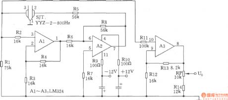
The circuit shown in the chart is 800Hz oscillator with the advantages of simple circuit, high accuracy of frequency and stable output level. It consists of four operational amplifiers Manifold Al ~ A3 (LM324) and the 800Hz oscillator composed of SJT (YYZ-2-800Hz) tuning fork. When 800Hz oscillation signal produced by SJ1 being added to two-stage operational amplifier formed by A1 and A2, it will be output by pin ⑦ and become positive feedback frequency signal through the resistor R5, SJT. Then the amplified 800Hz is amplified by A3 again. And it will be sent by pin ⑧ to the potentiometer RP, the adjustable arm can output (Uo) 800Hz sine wave signal. Among them, adjusting the potentiometer RP will meet the output level of 0dB/600Ω, adjustable range is ± 3db. (View)
View full Circuit Diagram | Comments | Reading(1262)
12kHz signal generator
Published:2011/4/20 4:28:00 Author:Ecco | Keyword: 12kHz, signal , generator
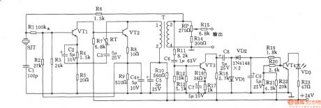
The 12kHz signal generator is shown as the chart, it is composed of the crystal oscillator and the alarm circuit. Oscillator output amplitude is stable, changing <± 0.26dB. Selection components: transistor VTl, VT3: 9014,65 ≤ β ≤ 115; VT2, VT4: 3DGl308, 60 ≤ β ≤ 85. Thermistor RT: RRWl-2 type. Crystal SJT: BE42-12kHz. The transformer T uses MXD-2000 ferrite, the core is GV36X22, Ll-2 uses Φ0.17mm high-strength wire with 57 turns, L3-4 uses Φ0.17mm high-strength wire with 37 turns. Models of light-emitting diode VD3 is not limited. Nominal power of resistor selects 1/8W metal film resistors. Other component values are shown in Figure, there's no special requirements.
(View)
View full Circuit Diagram | Comments | Reading(779)
Various waveforms generator
Published:2011/4/20 21:27:00 Author:Ecco | Keyword: Various , waveform , generator
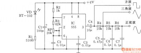
The circuit shown as the chart, it can produce square wave, triangle wave, sine wave and output at the same time, it is especially for the electronic hobbyist or student to do oscilloscope waveform observation experiments. The signal generator circuit is simple, low-cost, easy to adjust. 555 timer connecting as a multivibrator, C2 is the timing capacitor, the charging circuit of C2 is R2 → R3 → RP → C2; C2 discharging circuit is C2 → RP → R3 → pin 7 of IC (discharging tube). The value of R3 + RP is higher than R2, so the charging and discharging time time constants is approximately equal, the pin 3 of IC outputs an approximately symmetrical square wave. Device parameters are as shown, the frequency is about 1kHz, adjusting potentiometer RP can change the oscillator frequency. Square-wave signal becomes triangular wave by the R4, C5 integration network. Triangle wave becomes sine wave by R5, C6 integral network. C1 is the power supply filter capacitor . The light-emitting diode VD is used as power indicator. (View)
View full Circuit Diagram | Comments | Reading(10567)
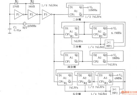
Crystal oscillator and divider(74LS04)
Published:2011/4/20 7:02:00 Author:Ecco | Keyword: Crystal oscillator , divider
View full Circuit Diagram | Comments | Reading(1776)
RC sine-wave generator composed of LM741CN
Published:2011/4/20 21:40:00 Author:Ecco | Keyword: RC , sine-wave generator
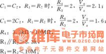
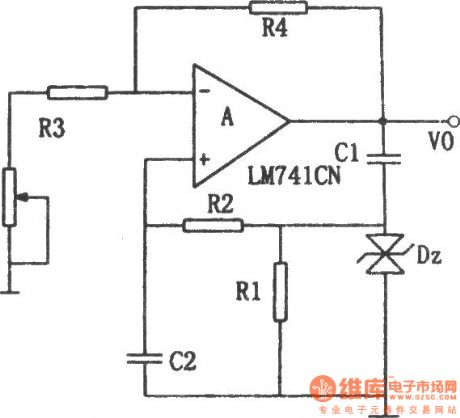
The chart shows the RC sine-wave generator. The components can be selected according to the following formula:
(View)
View full Circuit Diagram | Comments | Reading(2327)
Beijing grand cherokee car charging marine system circuit diagram
Published:2011/4/26 2:11:00 Author:Rebekka | Keyword: Beijing grand cherokee, car charging marine system
Beijing grand cherokee car charging marine system circuit diagram is shown as above. (View)
View full Circuit Diagram | Comments | Reading(503)
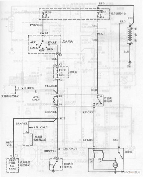
Beijing grand cherokee car start system circuit diagram 3
Published:2011/4/26 2:09:00 Author:Rebekka | Keyword: Beijing grand cherokee car, start system
Beijing grand cherokee car start system circuit diagram is shown as above. (View)
View full Circuit Diagram | Comments | Reading(738)
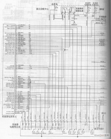
Beijing grand cherokee car automatic transmission circuit diagram 3
Published:2011/4/26 2:08:00 Author:Rebekka | Keyword: Beijing grand cherokee car, automatic transmission

Beijing grand cherokee car automatic transmission circuit diagram is shown as above. (View)
View full Circuit Diagram | Comments | Reading(808)
Beijing grand cherokee car engine circuit diagram 3
Published:2011/4/26 2:01:00 Author:Rebekka | Keyword: Beijing grand cherokee, car engine
Beijing grand cherokee car engine circuit diagram is shown as below. (View)
View full Circuit Diagram | Comments | Reading(500)
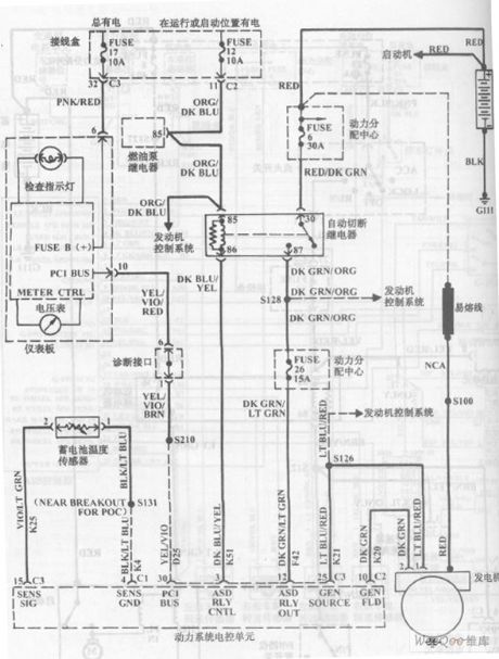
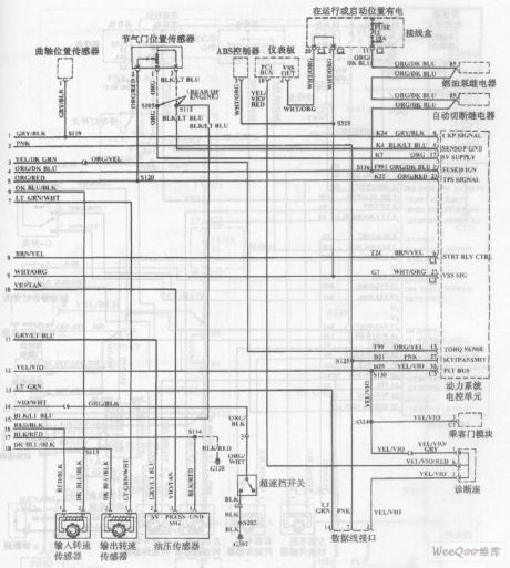
Beijing grand cherokee car dynamic transmission circuit diagram 1
Published:2011/4/26 2:03:00 Author:Rebekka | Keyword: Beijing grand cherokee car , dynamic transmission
Beijing grand cherokee car dynamic transmission circuit diagram is shown as above. (View)
View full Circuit Diagram | Comments | Reading(529)
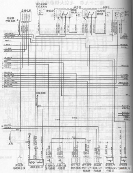
Beijing grand cherokee car dynamic transmission circuit diagram 2
Published:2011/4/26 2:04:00 Author:Rebekka | Keyword: Beijing grand cherokee , car dynamic transmission
Beijing grand cherokee car dynamic transmission circuit diagram is shown as above. (View)
View full Circuit Diagram | Comments | Reading(476)
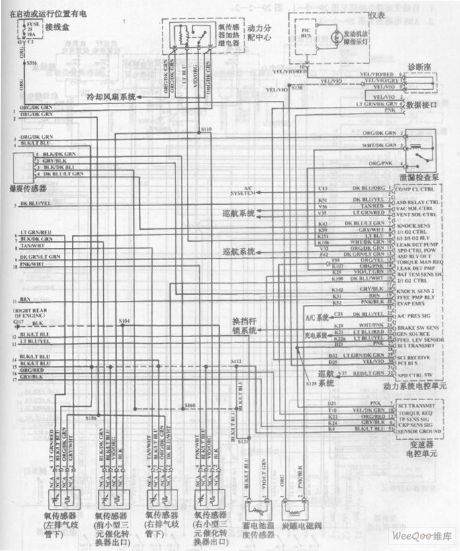
Beijing grand cherokee car engine circuit diagram 2
Published:2011/4/26 2:00:00 Author:Rebekka | Keyword: Beijing grand cherokee, car engine
Beijing grand cherokee car engine circuit diagram is shown as below. (View)
View full Circuit Diagram | Comments | Reading(585)
Using DTMF encoding and decoding wireless calling implement circuit diagram
Published:2011/4/24 10:59:00 Author:Rebekka | Keyword: DTMF , encoding and decoding , wireless calling implement


The wireless calling implement is composed of calling implement and the host. The two parts use DTMF encoder pulse to realise communication. Different calling implement has different codes only, the circuits are all the same. The calling implement is shown in figure 1. IC2 is the DTMF encoding specific integrated circuit (telephone dial tone can also be integrated circuits), which has four southbound R1 ~ R4, C1 ~ C4 line of four columns, external standard 4 × 4 matrix keyboard. It produces 16 different encoding. When any key is pressed, a row line and a column line are connected. Then the output pin corresponding to the end TONE tone pulses. It uses optocoupler number keys as the icon to connect to 1 # key. IC3 serial data of the long-wave radio transmitter module, which uses 150kHz carrier frequency, a strong anti-interference ability. IC2 pin dual audio pulses emitted modulated carrier out by the antenna.
(View)
View full Circuit Diagram | Comments | Reading(2304)
300kHz Signal generator
Published:2011/4/21 5:32:00 Author:Ecco | Keyword: 300kHz , Signal generator
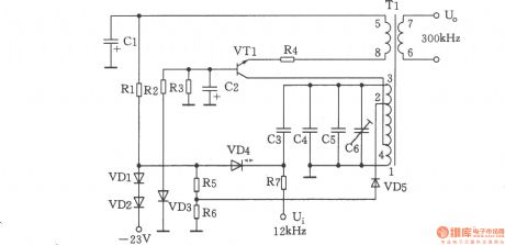
The chart shows the 300kHz signal generator. It is a voltage-controlled oscillator which is composed of VT1, T1, VD4 and related components. VCO use LC tuned collector, VTl is the oscillating tube, the 1 to 3 inductor winding of varactor diode VD4, and the capacitors C3 ~ C6 and transformer T1 form a tuning loop, the back biased work of varactor diode VD4 can control voltage which is applied to the negative side, and it can change its electrical capacity. The oscillating signal is from the output windings 6 to 7 of Tl. And C6 is the frequency tuning capacitor. VD3 stablizes oscillation voltage level, stable voltage is 6.8V ± 0.2V. Selection of components: transistor VT1: 3DG6C, β = 65 ~ 85. Diode VD1, VD2: 2CPl4, VD5: 2CK18. Zener diode VD3: 2CWl4. Varactor diode VD4: 2CC5. Resistor R1: 3.6k, R2: 3.3k, R3: 5.1k, R4: 510Ω, R5: 3.9k, R6: 3k, R7: 100k, the models are RTX-0.125W. Capacitors Cl, C2: 5μF30V, C3: 51pFl00V, C4: 820pFl00V, C5: (matching when measuring), C6: 20pF. Variable device T1: model L22, A = 100. L1-4: Φ0.29mm, around 27 turns, L2-3: Φ0.29mm, turn around l8, L4-2: Φ0.29ram with 9 turns, L5-8: Φ0.29mm with 7 turns, L6- 7: ΦO. 29mm with 6 turns. L1-3 = 292μH, allowable error range: 0 ~ 10μH. (View)
View full Circuit Diagram | Comments | Reading(1107)
70MHz parallel crystal oscillator
Published:2011/4/20 22:47:00 Author:Ecco | Keyword: 70MHz, parallel, crystal oscillator
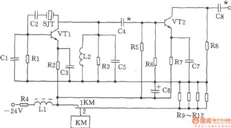
The chart shows 70MHz parallel crystal oscillator circuit. The oscillator is mainlycomposed ofthe transistor VTl, crystal SJT and capacitor Cl, C5 and other components. Selection ofcomponents: capacitors Cl, 20p, C2 to 100p, C3, C7 to 820p, C4 to 56p, C5, C8 to 47p, C6 to 47μF/50V. Inductor Ll is 22μH (color code inductance), L2 is 0.3μH. Resistor Rl is 1.6kΩ, R2 is 1kΩ, R3 is 750Ω, R4 is 180Ω, 1W, R5 is 1.3kΩ, R6 is 3kΩ, R7 is 360Ω, R8 is 470Ω, R9 ~ R12 is 300Ω, 2W. Transistor VTl, VT2choose 3DG828, 65 ≤ β ≤ 115. Crystal SJTchooses JA98-70MHz. Relay KM is JUC-1M.
(View)
View full Circuit Diagram | Comments | Reading(834)
| Pages:186/195 At 20181182183184185186187188189190191192193194195 |
Circuit Categories
power supply circuit
Amplifier Circuit
Basic Circuit
LED and Light Circuit
Sensor Circuit
Signal Processing
Electrical Equipment Circuit
Control Circuit
Remote Control Circuit
A/D-D/A Converter Circuit
Audio Circuit
Measuring and Test Circuit
Communication Circuit
Computer-Related Circuit
555 Circuit
Automotive Circuit
Repairing Circuit