Want to post a buying lead? If you are not a member yet, please select the specific/related part number first and then fill the quantity and your contact details in the "Request for Quotation Form" on the left, and then click "Send RFQ".Your buying lead can then be posted, and the reliable suppliers will quote via our online message system or other channels soon.
This improved version of MDmesh™ which is based on Multiple Drain process represents the new benchmark in high voltage MOSFETs. The resulting product exhibits even lower on-resistance, impressively high dv/dt and excellent avalanche characteristics. The adoption of the Company's proprietary strip technique yields overall performances that are significantly better than that of similar competition's products.
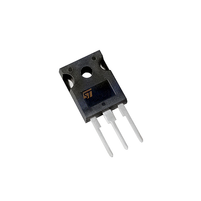
STW22NM60 Maximum Ratings
Symbol
Parameter
Value
Unit
STP22NM60 STB22NM60/1
STF22NM60
STW22NM60
VDS
Drain-source Voltage (VGS = 0)
600
V
VDGR
Drain-gate Voltage (RGS = 20 k)
600
V
VGS
Gate- source Voltage
± 30
V
ID
Drain Current (continuos) at TC = 25
22
22(*)
22
A
ID
Drain Current (continuos) at TC = 100
12.6
12.6(*)
12.6
A
IDM()
Drain Current (pulsed)
80
80(*)
80
A
PTOT
Total Dissipation at TC = 25
192
45
210
W
Derating Factor
1.2
0.36
1.2
W/
dv/dt (1)
Peak Diode Recovery voltage slope
15
V/ns
VISO
Insulation Withstand Voltage (DC)
-
2500
-
V
Tstg
Storage Temperature
-65 to 150
Tj
Max. Operating Junction Temperature
150
() Pulse width limited by safe operating area; (*)Limited only by maximum temperature allowed (1) ISD22A, di/dt400A/s, VDD V(BR)DSS, Tj TJMAX
STW22NM60 Features
` TYPICAL RDS(on) = 0.19 ` HIGH dv/dt AND AVALANCHE CAPABILITIES ` 100% AVALANCHE TESTED ` LOW INPUT CAPACITANCE AND GATE CHARGE ` LOW GATE INPUT RESISTANCE
STW22NM60 Typical Application
The MDmesh™ family is very suitable for increasing power density of high voltage converters allowing system miniaturization and higher efficiencies.
The STx25NM50N is realized with the second generation of MDmesh Technology. This revolutionary MOSFET ssociates a new vertical structure to the Company's strip layout to yield one of the world's lowest on-resistance and gate charge. It is therefore suitable for the most demanding high efficiency converters.
STW25NM50N Maximum Ratings
Symbol
Parameter
Value
Unit
TO- 220/D²PAK/ I²PAK/TO-247
TO-220FP
VDS
Drain-source Voltage (VGS = 0)
500
V
VDGR
Drain-gate Voltage (RGS = 20 k)
500
V
VGS
Gate- source Voltage
± 25
V
ID
Drain Current (continuos) at TC = 25
22
22(*)
A
ID
Drain Current (continuos) at TC = 100
14
14(*)
A
IDM()
Drain Current (pulsed)
88
88(*)
A
PTOT
Total Dissipation at TC = 25
160
40
W
Derating Factor
1.28
0.32
W/
dv/dt (1)
Peak Diode Recovery voltage slope
15
V/ns
Tstg
Storage Temperature
55 to 150
Tj
Max. Operating Junction Temperature
150
() Pulse width limited by safe operating area (1) ISD 22A, di/dt 400A/s, VDD 80% V(BR)DSS. (*) Limited only by maximum temperature allowed
STW25NM50N Features
· HIGH dv/dt AND AVALANCHE CAPABILITIES · 100% AVALANCHE TESTED · LOW INPUT CAPACITANCE AND GATE CHARGE · LOW GATE INPUT RESISTANCE
STW25NM50N Typical Application
The MDmesh™ II family is very suitable for increasing power density of high voltage converters allowing system iniaturization and higher efficiencies.
The STP25NM60N is realized with the second generation of MDmesh Technology. This revolutionary MOSFET associates a new vertical structure to the Company's strip layout to yield the world's lowest on-resistance and gate charge. It is therefore suitable for the most demanding high efficiency converters
STW25NM60N Maximum Ratings
Symbol
Parameter
Value
Unit
TO-220/I²PAK TO-247/D²PAK
TO-220FP
VDS
Drain-source Voltage (VGS = 0)
600
V
VDGR
Drain-gate Voltage (RGS = 20 k)
600
V
VGS
Gate- source Voltage
±25
V
ID
Drain Current (continuos) at TC = 25
20
20(*)
A
ID
Drain Current (continuos) at TC = 100
12.8
12.8(*)
A
IDM(1)
Drain Current (pulsed)
80
80(*)
A
PTOT
Total Dissipation at TC = 25
160
40
W
Derating Factor
1.28
0.32
W/
dv/dt (2)
Peak Diode Recovery voltage slope
TBD
V/ns
Tstg
Storage Temperature
55 to 150
Tj
Max. Operating Junction Temperature
150
(*) Limited only by maximum temperature allowed (1) Pulse width limited by safe operating area (2) ISD 20 A, di/dt 400 A/s, VDD =80%V(BR)DSS.
STW25NM60N Features
` WORLD'S LOWEST ON RESISTANCE ` TYPICAL RDS(on) = 0.140 ` HIGH dv/dt AND AVALANCHE CAPABILITIES ` 100% AVALANCHE TESTED ` LOW INPUT CAPACITANCE AND GATE CHARGE ` LOW GATE INPUT RESISTANCE
STW25NM60N Typical Application
The MDmesh™ II family is very suitable for increase the power density of high voltage converters allowing system miniaturization and higher efficiencies .