Want to post a buying lead? If you are not a member yet, please select the specific/related part number first and then fill the quantity and your contact details in the "Request for Quotation Form" on the left, and then click "Send RFQ".Your buying lead can then be posted, and the reliable suppliers will quote via our online message system or other channels soon.
Using the latest high voltage MESH OVERLAYTM process, SGS-Thomson has designed an advanced family of power MOSFETs with outstanding performances. The new patent pending strip layout coupled with the Company's proprietary edge termination structure, gives the lowest RDS(on) per area, exceptional avalanche and dv/dt capabilities and unrivalled gate charge and switching characteristics.
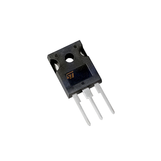
STW5NB100 Maximum Ratings
Symbol
Parameter
Value
Unit
VDS
Drain-source Voltage (VGS = 0)
1000
V
VDGR
Drain- gate Voltage (RGS = 20 k)
1000
V
VGS
Gate-source Voltage
±30
V
ID
Drain Current (continuous) at Tc = 25
4.3
A
ID
Drain Current (continuous) at Tc = 100
2.7
A
IDM(•)
Drain Current (pulsed)
17
A
PTOT
Total Dissipation at Tc = 25
160
W
Derating Factor
1.28
W/
dv/dt(1)
Peak Diode Recovery voltage slope
4
V/ns
Tstg
Storage Temperature
-65 to 150
Tj
Max. Operating Junction Temperature
150
(•)Pulse width limited by safe operating area (1)ISD 4A, di/dt 200A/µs, VDD V(BR)DSS, Tj TJMAX.
STW5NB100 Typical Application
· HIGH CURRENT, HIGH SPEED SWITCHING · SWITCH MODE POWER SUPPLY (SMPS) · DC-AC CONVERTER FOR WELDING EQUIPMENT AND UNINTERRUPTABLE POWER SUPPLY AND MOTOR DRIVE
The SuperMESHTM series is obtained through an extreme optimization of ST's well establishe stripbased PowerMESH? layout. In addition to pushing on-resistance significantly down, special care is taken to ensure a very good dv/dt capability for the most demanding applications. Such series complements ST full range of high voltage MOS- FETs including revolutionary MDmeshTM products.
STW5NK100Z Maximum Ratings
Symbol
Parameter
Value
Unit
STP5NK100Z STW5NK100Z
STF5NK100Z
VDS
Drain-source Voltage (VGS = 0)
1000
V
VDGR
Drain-gate Voltage (RGS = 20 )
1000
V
VGS
Gate- source Voltage
±30
V
ID
Drain Current (continuous) at TC = 25
3.5
3.5(*)
A
ID
Drain Current (continuous) at TC = 100
2.2
2.2(*)
A
IDM(`)
Drain Current (pulsed)
15
14(*)
A
PTOT
Total Dissipation at TC = 25
125
30
W
Derating Factor
1
0.24
W/
VESD(G-S)
Gate source ESD(HBM-C=100pF, R=1.5K)
4000
V
dv/dt(1)
Peak Diode Recovery voltage slope
4.5
V/ns
VISO
Insulation Withstand Voltage (DC)
2500
V
Tj Tstg
Operating Junction Temperature Storage Temperature