Want to post a buying lead? If you are not a member yet, please select the specific/related part number first and then fill the quantity and your contact details in the "Request for Quotation Form" on the left, and then click "Send RFQ".Your buying lead can then be posted, and the reliable suppliers will quote via our online message system or other channels soon.
The third generation of MESH OVERLAY™ Power MOSFETs for very high voltage exhibits unsurpassed on-resistance per unit area while integrating back-to-back Zener diodes between gate and source. Such arrangement gives extra ESD capability with higher ruggedness performance as requested by a large variety of single-switch applications.
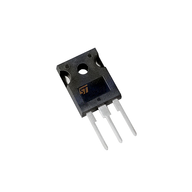
STW7NC80Z Maximum Ratings
Symbol
Parameter
Value
Unit
VDS
Drain-source Voltage (VGS = 0)
800
V
VDGR
Drain- gate Voltage (RGS = 20 k)
800
V
VGS
Gate-source Voltage
±25
V
ID
Drain Current (continuous) at Tc = 25
6
A
ID
Drain Current (continuous) at Tc = 100
3.8
A
IDM(•)
Drain Current (pulsed)
24
A
PTOT
Total Dissipation at Tc = 25
160
W
Derating Factor
1.28
W/
IGS
Gate-source Current (*)
±50
mA
VESD(G-S)
Gate source ESD(HBM-C=100pF, R=15K)
3
KV
dv/dt(1)
Peak Diode Recovery voltage slope
3
V/ns
Tstg
Storage Temperature
-65 to 150
Tj
Max. Operating Junction Temperature
150
(•)Pulse width limited by safe operating area (1)ISD 6A, di/dt 100A/µs, VDD V(BR)DSS, Tj TJMAX.
STW7NC80Z Features
The built-in back-to-back Zener diodes have specifically been designed to enhance not only the device's ESD capability, but also to make them safely absorb possible voltage transients that may occasionally be applied from gate to souce. In this respect the 25V Zener voltage is appropiate to achieve an efficient and cost-effective intervention to protect the device's integrity. These integrated Zener diodes thus avoid the usage of external components.
STW7NC80Z Typical Application
· SINGLE-ENDED SMPS IN MONITORS,COMPUTER AND INDUSTRIAL APPLICATION · WELDING EQUIPMENT