Want to post a buying lead? If you are not a member yet, please select the specific/related part number first and then fill the quantity and your contact details in the "Request for Quotation Form" on the left, and then click "Send RFQ".Your buying lead can then be posted, and the reliable suppliers will quote via our online message system or other channels soon.
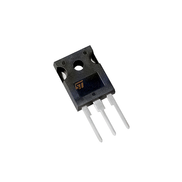
Using the well consolidated high voltage MESH OVERLAY™ process, STMicroelectronics has designed an advanced family of Power MOSFETs with outstanding performances. The strengthened layout coupled with the Company's proprietary edge termination structure, gives the lowest RDS(on) per area, unrivalled gate charge and switching characteristics.
STW9N150 Maximum Ratings
Symbol
Parameter
Value
Unit
VDS VGS ID ID IDM(1) PTOT
Tj Tstg
Drain-source voltage (VGS = 0) Gate- source voltage Drain current (continuous) at TC = 25°C Drain current (continuous) at TC = 100°C Drain current (pulsed) Total dissipation at TC = 25°C Derating factor
Operating junction temperature Storage temperature
1500 ± 30 8 5 32 350 0.37
55 to 150
V V A A A W W/°C
°C
STW9N150 Features
100% avalanche tested Avalanche ruggedness Gate charge minimized Very low intrinsic capacitances High speed switching Very low on-resistance