
A/D-D/A Converter Circuit
Index 24
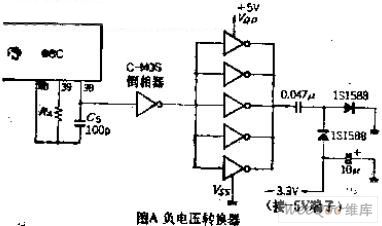
Bridge type voltage converter circuit
Published:2011/7/10 18:56:00 Author:TaoXi | Keyword: Bridge type, voltage converter
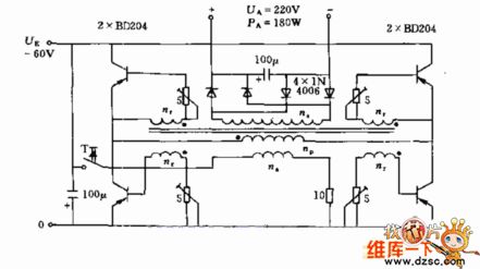
Figure:Bridge type voltage converter circuit
(View)
View full Circuit Diagram | Comments | Reading(806)
Voltage converter circuit uses the RC link to produce the control frequency
Published:2011/7/10 18:58:00 Author:TaoXi | Keyword: Voltage converter, RC link, control frequency
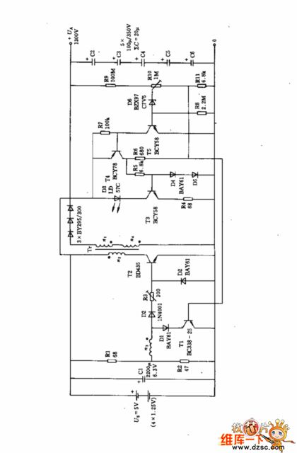
Figure:Voltage converter circuit uses the RC link to produce the control frequency
(View)
View full Circuit Diagram | Comments | Reading(773)
RS232-485 conversion circuit
Published:2011/7/6 2:57:00 Author:Christina | Keyword: conversion circuit
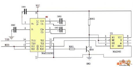
The RS232-485 conversion circuit is as shown:
(View)
View full Circuit Diagram | Comments | Reading(1331)
555 TV programs monitoring and timing conversion circuit
Published:2011/6/16 1:11:00 Author:TaoXi | Keyword: 555, TV programs, monitoring, timing, conversion circuit
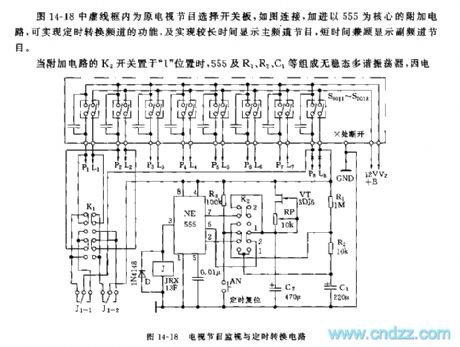
When the switch K2 of the additional circuit is in the position 1 , the astable multivibrator is composed of the 555 and R1, R2, C1, because the charging time of the circuit tcharging=0.693(R1+R2)C1, it is larger than the discharging time td=0.693R2C1, so the duty ratio of the output pulse is small, this circuit can realize the main channel long-time display (about 10 minutes) and the vice channel short display (about 5 seconds). When the K2 is in the position 2 , the monostable timing circuit is composed of the 555 and R3, VT, RP, C2. The constant current source is composed of the MOSFET 3DJ6, this constant current source charges the C2 to improve the timing accuracy. By adjusting RP, you can pre-set the timing time (5 to 90 minutes). When this circuit is used as the timing circuit, you need to press AN to set the 555 circuit, so the timing starts.
(View)
View full Circuit Diagram | Comments | Reading(733)
Thyristor parallel connection inverter circuit
Published:2011/7/3 20:42:00 Author:Christina | Keyword: Thyristor, parallel connection, inverter circuit
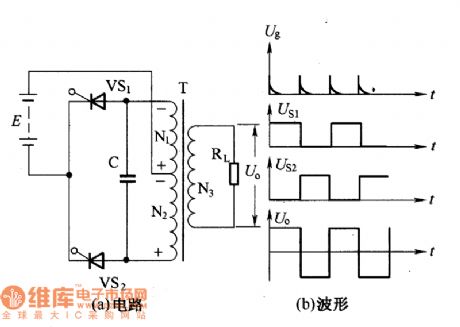
The circuit is as shown in the figure, it is composed of two unidirectional thyristors, the transformer, the reversing capacitance and the load resistance. The reversing capacitance C and the primary equivalent load are in the parallel connection, the E is the DC input power supply.
When the circuit is operating, the control signal Ug triggers the two thyristors VS1 and VS2 alternately. If the VS1 is triggered and conducted, and the VS2 is in the cut-off state, so the current will be back to the negative electrode from the DC power supply positive electrode through the primary windings N1 and VS1 of the transformer T. The primary winding N2 produces the induced voltage E, the voltage of N1 and N2 charges the C, so the voltage of C is Uc=2E.
(View)
View full Circuit Diagram | Comments | Reading(4167)
Thyristor ladder wave inverter circuit
Published:2011/7/3 20:25:00 Author:Christina | Keyword: Thyristor, ladder wave, inverter circuit
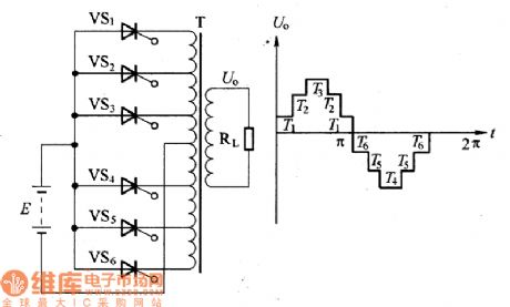
The circuit is as shown, the six taps of the transformer T is connected with the unidirectional thyristors VS1~VS6 to form the thyristor inverter main circuit.
By the function of the trigger control circuit, the action program of the circuit is as shown: the circuit makes the thyristor VS1 to conduct for 30°, then it makes the VS2 to conduct for 30°, then makes the VS3 to conduct for 60°, during this time the thyristors cuts off by the induced voltage which is produced by the transformer winding. After the VS3 cuts off, the circuit will cut off the VS2 to finish the output of the half cycle ladder wave.
Thyristor ladder wave inverter circuit (View)
View full Circuit Diagram | Comments | Reading(5265)
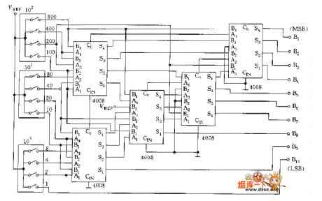
BCD binary number convert circuit diagram
Published:2011/6/24 8:23:00 Author:Nicole | Keyword: binary, number, convert
View full Circuit Diagram | Comments | Reading(5075)
B0505LM-1W DC/DC converter application circuit
Published:2011/6/21 8:13:00 Author:TaoXi | Keyword: DC/DC, converter, application circuit
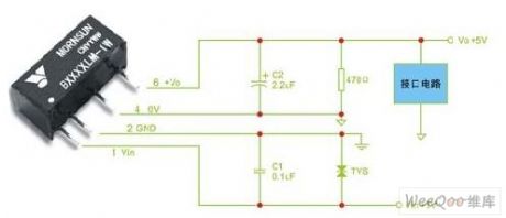
The B0505LM-1W series products are produced by the MORNSUN company, the B0505LM-1W series products are very suitable in this project, the B0505LM-1W is a 1000VDC subminiature DC/DC converter with good reliability, the input voltage is 5V, the output voltage is 5V, the power is 1W, the typical application circuit is as shwon in figure 1. Because this device has the 1000VDC isolation between the input and output, and the output short circuit time is 1 second, so it can resist the interference of the high frequency transient impulse.
By improving the technology, the reliability of the MORNSUN products are better and better. Meanwhile the quality engineer strictly controls the supplier selection and the incoming quality control (IQC).
Figure 1 The typical application circuit of the B0505LM-1W (View)
View full Circuit Diagram | Comments | Reading(1309)
1.5V battery power supply 15V output DC/DC booster circuit
Published:2011/6/21 21:16:00 Author:TaoXi | Keyword: 1.5V, battery, power supply, 15V, output, DC/DC, booster
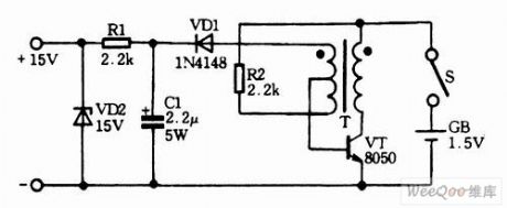
1.5V battery power supply 15V output DC/DC booster circuit (View)
View full Circuit Diagram | Comments | Reading(6250)
Temperature sensor A/D converter circuit
Published:2011/6/22 20:56:00 Author:TaoXi | Keyword: Temperature sensor, A/D, converter
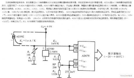
In the microcontroller temperature measurement system, you need to change the analog quantity of the AD592 into the digital quantity through the A/D converter, then the digital quantity is sent to the single-chip microcomputer to be processed. The A/D converter circuit of the AD592 is as shown in the figure, this circuit uses the AD670 for the 8-bit A/D conversion. The AD670 belongs to the 4-port differential input, it is designed as the 8-bit A/D converter which is composed of the input attenuator, the measurement amplifier and the reference voltage source. The four analog input ports are divided into two groups, every group has the attenuator which is composed of the 1kΩ and 10kΩ resistance.
(View)
View full Circuit Diagram | Comments | Reading(1487)
555 TV double-channel monitoring automatic conversion circuit
Published:2011/6/15 2:19:00 Author:TaoXi | Keyword: 555, TV, double-channel, monitoring, automatic conversion
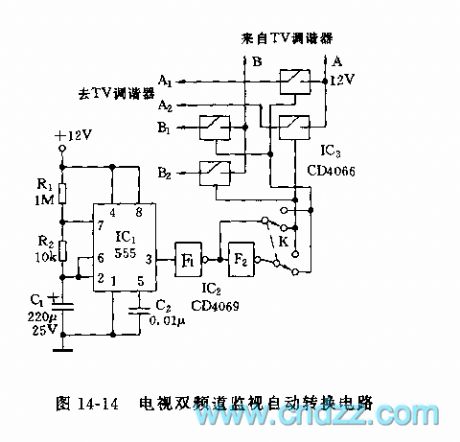
As the figure 14-14 shows, the conversion circuit is composed of the high duty ratio square-wave generator and the electronic switch, it can be used in the automatic conversion of the two TV channels.
The astable multivibrator is composed of the 555 and R1, R2, C1, because the R1>>R2, so the duty ratio is 99%. The IC2 is the six-inverter CD4069. The IC3 which can be used as the inverter phase control electronic switching circuit of the two channels uses the 4-channel analog switch CD4066. It divides the switches into two groups, one group controls the power supply voltage A1 and tuning voltage B1 of the main channel; another group controls the power supply voltage A2 and the tuning voltage B2 of the monitor channel. K is the 2X2 switch that can be used to select the main and auxiliary channels.
(View)
View full Circuit Diagram | Comments | Reading(862)
Low-power liquid crystal display 3 1/2 A-D converter circuit
Published:2011/6/3 20:53:00 Author:Fiona | Keyword: Low-power liquid crystal display
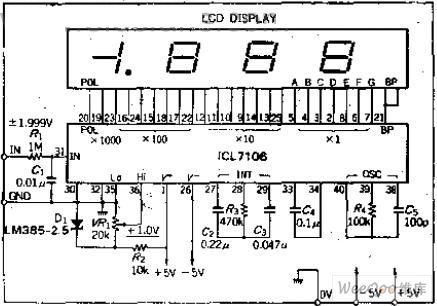
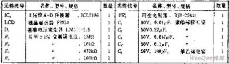
Circuit function
This is a digital display type A-D converter.It is suitable for portable small measuring instrument. Because of the use of liquid crystal display andLow consumption, Full range display voltage is 1.999V. If the input voltage is greater than this value, it should be added a attenuator.The circuit is more used for measuring instrument.Its power source voltage is in positive and negative 5V.
Circuit Work
3 1 / 2-bit A-D converter ICL7106 is a monolithic LSI that can directly drive liquid crystal display, is general Instrument IC and other companies have processed products. A - D convert way is ordinary double integral type, differential input circuit can input positive and negative about 1V phase voltage, the internal does automatic zero set. Circuit adjustment can only use VR1.
(View)
View full Circuit Diagram | Comments | Reading(2446)
CXD2598Q-the integrated circuit of digital signal and servo processing with audio D/A converter
Published:2011/5/16 4:51:00 Author:Borg | Keyword: integrated circuit, digital signal, D/A converter
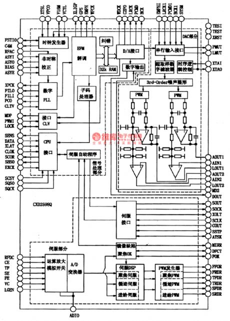
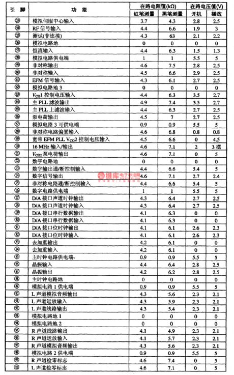
CXD2598Q is a very-large scale integrated circuit(VLSI) which produced by Sony Corp.. It is manufactured on the basis of CXD2585Q, which combines filters of 8 bit, 1 bit D/A converter and low-pass filter with digital signal processor and digital servo processing circuit. The circuit is widely used in Figure 1-1.1.Function featuresCXD2598Q digital signal processing circuit is fixed with digital PLL technology and super error-correcting algorithm, which can do EFM demodulation to the input RF signals. The internal circuit of if is shown in Figure 1.
(View)
View full Circuit Diagram | Comments | Reading(1173)
formed by common components 4 input 12-bit A-D converter diagram
Published:2011/5/11 3:23:00 Author:Fiona | Keyword: formed by common components, 4 input
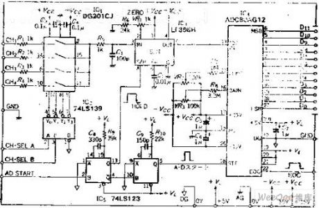
Circuit function
Recently, there is a variety of general-purpose AD conversion expansion board as a personal computer expanded with being sold on the market , if limited specific use, production costs can be low.
This circuit is a 12-bit AD converterusing in sample and hold circuits which is composed of the universal element and 4 inputs. It can enter positive and negative analog signals.
Circuit work
Analog input mux using the standard analog switch DG201, chooses 1~4 channel with decoder IC , channel selection input control by the two positive logic. After selecting channel, input about 10US wide sampling pulse to the sample and hold circuit to keep the analog voltage.The pulse starts to pulse by the AD pulse, using the pulse rising edge to begin 12-bit conversion. The conversion time is about 25US, 12-bit data output from D0 ~ D11. About EOC signal: when A-D conversion starts, EOC is H level and count the clock pulse.After conversion, EOC is back L level, so we can use the method of detecting EOC signai's rising and falling to read the slide 12-bit data.
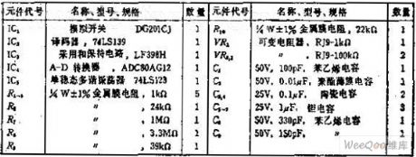
Component selection
(View)
View full Circuit Diagram | Comments | Reading(813)
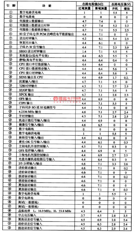
LC78816-two channel 16bit digit/model transformation integrated circuit diagram
Published:2011/5/6 2:40:00 Author:Nicole | Keyword: two channel, 16bit digit/model transformation
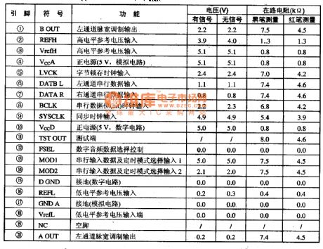
LC78816 is a two channel 16bit digit/model transformation integrated circuit which is special designed for processing the digital audio frequency singal, it is widely used in rear projection TV and digital audio system.
LC78816 contains two groups of independent dynamic state level migration converter, each group converter has 512 electric resistance belts, 3bit pulse width modulation circuit(PWM) and 4bit level migration circuit. It is used in Konka BT5O01 rear projection TV, in the digital convergence system, it is used as dynamic state digital convergence singal digit/model transformation, the pin function and data of this integrated circuit is shown in the table1.
(View)
View full Circuit Diagram | Comments | Reading(771)
TPS61042 DC/DC transformation integrated circuit diagram of adjustable LED brightness
Published:2011/5/5 22:47:00 Author:Nicole | Keyword: DC/DC transformation, adjustable LED brightness
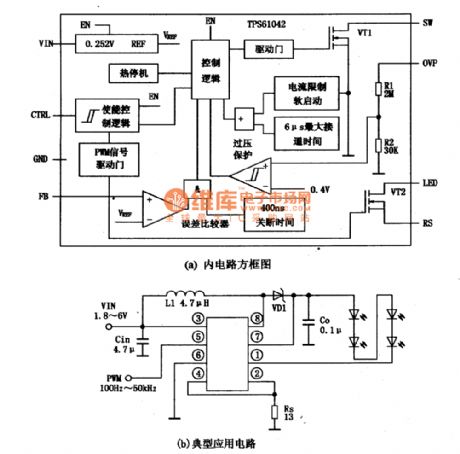
TPS61042 is a high-frequency control DC output LED driver which is produced by TI Texas Instrument. It is used in PDA, palm computer, hand-held devices and mobile phone devices.
1, internal circuit block diagram and typical application circuit
TPS61042 integrated block's internal circuit block diagram and typical application circuit is shown in the figure1-1(a), (b).
2, pin function
TPS61042 integrated circuit's pin function is shown in the table1-2.
(View)
View full Circuit Diagram | Comments | Reading(1095)
Electronic Video Switcher Circuit
Published:2011/4/24 22:21:00 Author:TaoXi | Keyword: Electronic Video, Switcher
The Electronic Video Switcher Circuit is as shown:
(View)
View full Circuit Diagram | Comments | Reading(2785)
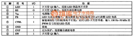
Power module transformation/Drive Circuit Diagram
Published:2011/3/21 4:17:00 Author:Nicole | Keyword: Power Module transformation, Drive Circuit Diagram
View full Circuit Diagram | Comments | Reading(673)
| Pages:24/24 At 2021222324 |
Circuit Categories
power supply circuit
Amplifier Circuit
Basic Circuit
LED and Light Circuit
Sensor Circuit
Signal Processing
Electrical Equipment Circuit
Control Circuit
Remote Control Circuit
A/D-D/A Converter Circuit
Audio Circuit
Measuring and Test Circuit
Communication Circuit
Computer-Related Circuit
555 Circuit
Automotive Circuit
Repairing Circuit