
A/D-D/A Converter Circuit
Index 21
SUCCESSIVE_APPROXIMATION_A_D_CONVERTER
Published:2009/6/24 1:36:00 Author:May
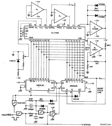
A bipolar input, high speed A/D converter uses two AM25L03s to form a 14-bit successive approximation register. The comparator is a two-stage circuit with an HA2605 front-end amplifier used to reduce settling time problems at the summing node. Careful offset-nulling of this amplifier is needed. (View)
View full Circuit Diagram | Comments | Reading(3)
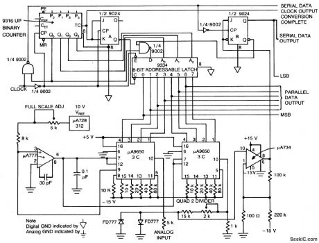
8_BIT_A_D_CONVERTER
Published:2009/6/24 1:33:00 Author:May
View full Circuit Diagram | Comments | Reading(0)
OCTAL_D_A_CONVERTER
Published:2009/6/23 2:00:00 Author:May
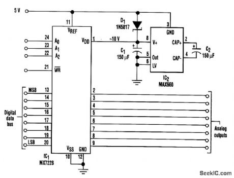
This octal digital-to-analog converter operates on 5V and provides eight output voltages, each digitally adjustable from supply rail to supply rail (0 to 5V). Each output's resolution is 20 mV/LSB. The DAC chip (IC1) requires 3.5V of headroom between its VDD and reference voltages. However, a voltage-doubler charge pump (IC2) removes this limitation by generating an approximate 10-V supply for VDD. All of the converter references are connected to the 5-V supply. IC2 doubles the 5-V input to an unregulated 10-V output that has an output impedance of less than 10Ω. It can deliver 100 rnA, which enables the eight DACs to issue their maximum output currents simultaneously (8×5 mA = 40 mA). (View)
View full Circuit Diagram | Comments | Reading(959)
ac_ISOLATION_TRANSFORMERS_USE_INEXPENSIVE_12_V_TRANSFORMERS
Published:2009/6/23 1:52:00 Author:May
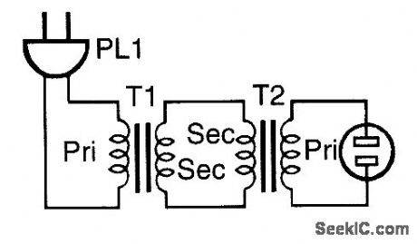
“Safety first”is a good motto to follow whenyou play vith electricity.You can follow thatadage more closely with this homebrew isolationtransformer (View)
View full Circuit Diagram | Comments | Reading(856)
OUTPUT_TO_CURRENT_CONVERTER
Published:2009/6/23 1:44:00 Author:May
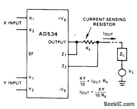
Occasionally, it is preferable to generate a cur-rent, rather than a voltage, output into the load.The availability of differential inputs aJlows this to be accomplished in any of the four basic modes.If the output is to integrated, ZL can be sim-ple high-quality capacitor, unloaded by an op amp connected as a high-impedance follower.Note that, if desired, one side of a rest switch can be grounded.The compliance constraint for this configura-tion, where VL is an arbitrary common-mode po-tential, is: |VL+IOUT(ZL+RS)|≤12V (View)
View full Circuit Diagram | Comments | Reading(0)
CURRENT_TO_VOLTAGE_CONVERTER_FOR_GROUNDED_LOADS
Published:2009/6/23 1:42:00 Author:May
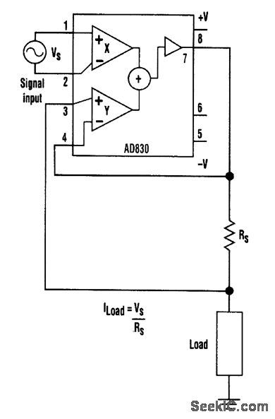
This circuit uses an Analog Devices AD830 video difference amplifier. The circuit consists of two differential inputs. Unlike a conventional op amp, the AD830's output is nulled when the sum of the differences of the two inputs is zero.The AD830's stated unity-gain bandwidth is 60 MHz, and the device is capable of driving up to ±30 mA directly. The differential input voltage is limited to ±2V, while the maximum power supply is ±15 V.If more output current is desired, the AD830 can drive a bipolar transistor (such as an MJE200) directly. This will produce a one-sided output.A ferrite bead can be placed on the base to prevent oscillation under some conditions. Com-pensation can be added by splitting RS, and adding a variable capacitor. A resistor can be po-sitioned at the input to match the amplifier's in-put to a transmission line. (View)
View full Circuit Diagram | Comments | Reading(0)
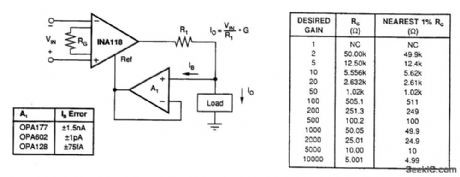
PROGRAMMABLE_CURRENT_TO_VOLTAGE_CONVERTER
Published:2009/6/23 1:38:00 Author:May
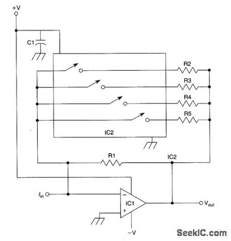
Programmable current-to-voltage converter permits you to electrically select from 16 resistor values using bilateral switches.
IC1 741 op amp (or similar)IC2 CD4066 quad bilateral switchC1 0.1-μF capacitorR1 10-kΩ 1/4-W 5% resistorR2 4.7-kΩ, 1/4-W 5% resistorR3 2.2-kΩ, 1/4-W 5% resistorR4 1.2-kΩ, 1/4-W 5% resistorR5 100-Ω, 1/4 5% resistor (View)
View full Circuit Diagram | Comments | Reading(1140)
LOW_FREQUENCY_CONVERTER
Published:2009/6/23 1:35:00 Author:May
This converter circuit translates the 350-to 500-kHz range to 4.35 to 4.50 MHz,enabling thefrequency range to be received on a conventionalshortwave recelver (View)
View full Circuit Diagram | Comments | Reading(1052)
DIFFERENTIAL_VOLTAGE_TO_CURRENT_CONVERTER
Published:2009/6/23 Author:May
View full Circuit Diagram | Comments | Reading(1188)
SYNC_TO_ASYNC_CONVERTER
Published:2009/6/22 23:58:00 Author:May
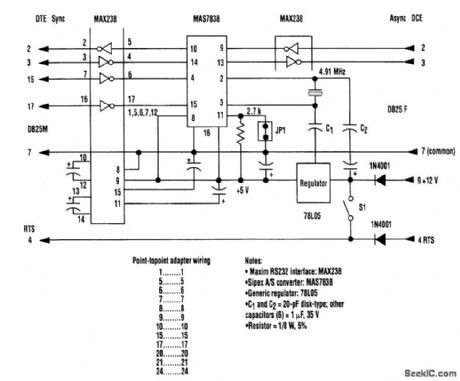
This simple converter donsists of two ICs and a voltage regulator. The Sipex MAS7838, which acts as the converter, selects the conversion speed to that of the synchronized data clock. It has intemal switches and registers to perform the async-to-sync, or sync-to-async, conversion. The Maxim MAX238 provides the RS-232 drivers and receivers for interfacing with the data bus. These chips require a 5-Vdc power supply; a generic 78L05 reduces the +12V at the DB25 pin 9 to the +5V needed. A crystal fre-quency of 4.91MHz is suitable for convetting to 19.2 kbits or a sub-multiple (9.6, 4.8, 2.4, etc.). Two 1N4001 diodes protect the extemal RTS (ready to send) control circuitry if the RTS is enabled by S1.When JP1 is removed, the converter is transparent in the sync mocte and no conversion will occur.The completed unit is mounted atop a universal breakout adapter, and the control lines are jumpered according to the chart in the figure. The physical size is approximately 1 x 2.25 x 2.5 inches and will easily plug into the DB25 socket on a synchronized data communications equipment (DCE) communication device. (View)
View full Circuit Diagram | Comments | Reading(1960)
5_V,5_A_STEP_DOWN_CONVERTER
Published:2009/6/22 23:56:00 Author:May


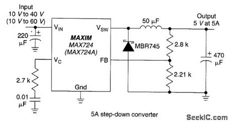
This circuit is useful where power must be distributed by a higher (10 to 60 V) bus. The circuit reduces power dissipation and elintinates inefficient passive linear regulators. The switching fre-quency is in the 100-kHz region. (View)
View full Circuit Diagram | Comments | Reading(861)
SCR_CONVERTER
Published:2009/6/22 23:55:00 Author:May
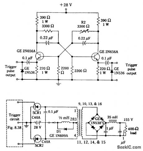
Two SCR devices are used in a push-pull driver to convert 28 Vdc to 155 Vdc, using the transformer and bridge shown. A center-tapped transformer with 24 V:120 V could be used for 60-Hz applications. The trigger circuit supplies a push-pull drive signal. (View)
View full Circuit Diagram | Comments | Reading(1752)
SINE_WAVE_CONVERTER
Published:2009/6/22 23:54:00 Author:May
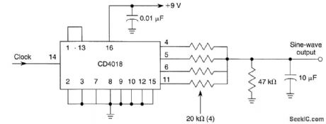
This circuit produces a sine wave with a low-frequency clock input. The clock rate should be 100Hz or less. (View)
View full Circuit Diagram | Comments | Reading(0)
DRIVEN_FLYBACK_CONVERTER
Published:2009/6/22 23:53:00 Author:May
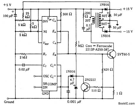
This circuit uses an SG1524 Silicon General regulating pulse width modulator and provides ±15 V from a 5-V supply rail. (View)
View full Circuit Diagram | Comments | Reading(0)
12_BIT_DAC
Published:2009/6/22 23:52:00 Author:May
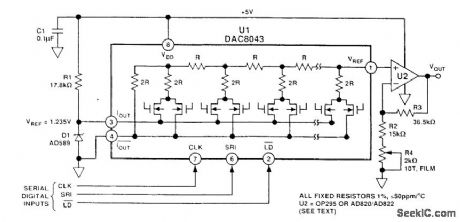
This circuit uses an Analog Devices DAC-8043 12-bit multiplying DAC The output will be D/4096×Vref where D is the numerical value of the digital input word(0 to 4095) Vref is 1.235 volts in this cicuit (View)
View full Circuit Diagram | Comments | Reading(0)
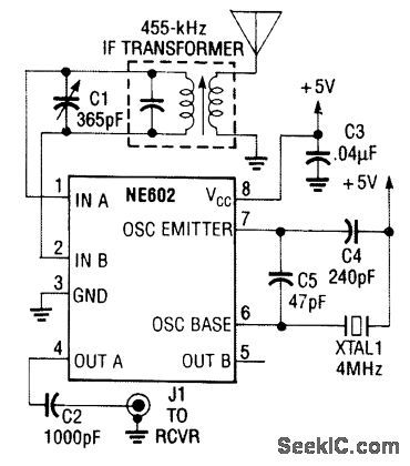
WWV_CONVERTER
Published:2009/6/22 23:37:00 Author:May
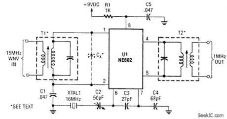
This converter heterodynes the 15-MHz WWW signal with a 16-MHz oscillator so that it can be heard at 1 MHz on an ANI broadcast receiver. T1 and T2 are a modified 10.7-MHz IF transformer and AM BO oscillator coil, respectively. (View)
View full Circuit Diagram | Comments | Reading(0)
RS_422_TO_RS_232_CONVERTER
Published:2009/6/22 22:52:00 Author:May
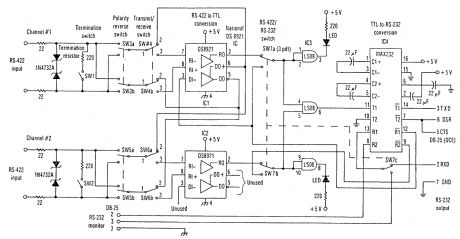
The circuit supplies two LEDs for visual indication of line activity and terminating resistors when needed. The 220-Q resis-tors and 5-V zeners at the RS-422 line inputs supply circuit protection.Switch SW7 allows the circuit monitor both transmitted and received signals when tee-connected into an RS-232 line. One function of this optional feature is the ability to test a software-locking device that connects to the COM1 port on an IBM PC. (View)
View full Circuit Diagram | Comments | Reading(3255)
BUFFER_FOR_A_D_CONVERTERS
Published:2009/6/22 22:47:00 Author:May
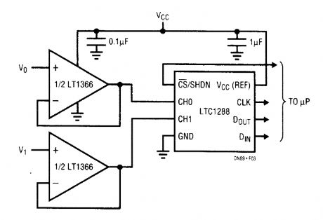
This circuit uses an LT1366 driving an LTC1288 two-channel micropower A/D. The LTC1288 can accommodate voltage references and input signals equal to the supply rails. The sampling nature of this A/D eliminates the need for an external sample-and-hold, but might call for a drive amplifier be-cause of the A/D's 12-ps settling requirement. The LT1366's rail-to-rail operation and low-input off-set voltage make it well suited for low-power, low-frequency A/D applications. In addition, the op-amp's output settles to 1% in response to a 3-mA load step through 100 pF in less than 1.5μs. (View)
View full Circuit Diagram | Comments | Reading(0)
FREQUENCY_TO_VOLTAGE_CONVERTER
Published:2009/6/19 3:04:00 Author:May

The AD537 can also be used to perform frequency-to-voltage conversion. The transistor pair shown here operates as an exclusive-or gate to perform the phase comparison. It locks onto the input frequency within two cycles. The configuration requires only 3 mA for frequencies up to 10 kHz. In most situations, an output buffer will be required to unload the filter. Use 0-to 5-V pulses or square waves with 40-μs minimum pulsewidth. (View)
View full Circuit Diagram | Comments | Reading(2)
INDUSTRIAL_FREQUENCY_TO_VOLTAGE_CONVERTER
Published:2009/6/19 3:02:00 Author:May

Control and process equipment often require the indication of frequency (speed or rate) of linear or rotary mechanical movement. Motion can be detected using various pulse-generating pickups and proximity detectors that output ac or dc pulsed signals.This industrial converter can serve in a wide variety of applications. The circuit operates around a quad-FET input op amp and is designed to be selfcontained or run from a bipolar supply. The in-put signal of dc pulses or ac waveforms is applied to R2.Amplifier 1, which acts as a Schmitt trigger, supplies a squarewave output of fixed amplitude to C4. Resistor R3 and capacitor C6 filter out input noise, and R4 and R5 determine the switching levels, and Zener diode 23 sets the amplitude.Amplifier 2 gives a fixed-duration pulse on the positive transition of C4, with a time constant set by C4 and R6 and the switching level set by R7 and R8. Resistor R9 and Zener diode 22 fix the am-plitude of the pulses and amplifier 3 integrates them via R10 and C5. Diode D6 blocks negative inte-gration and R11 discharges C5 with a long-time constant.Hence, the dc output of amplifier 3 is proportional to the frequency applied to the input. Amplifier 4 inverts and buffers the negative output of amplifier 3 and provides amplitude adjustment voltage.The complete circuit is linear and sufficiently accurate providing that C4 is chosen to give a pulse duration less than the maximum input frequency and that R11 > R10. (View)
View full Circuit Diagram | Comments | Reading(1076)
| Pages:21/24 At 2021222324 |
Circuit Categories
power supply circuit
Amplifier Circuit
Basic Circuit
LED and Light Circuit
Sensor Circuit
Signal Processing
Electrical Equipment Circuit
Control Circuit
Remote Control Circuit
A/D-D/A Converter Circuit
Audio Circuit
Measuring and Test Circuit
Communication Circuit
Computer-Related Circuit
555 Circuit
Automotive Circuit
Repairing Circuit