
A/D-D/A Converter Circuit
Index 22
SCHMITT_TRIGGER_OR_SINE_TO_SQUARE_WAVE_CONVERTER
Published:2009/6/18 23:29:00 Author:May
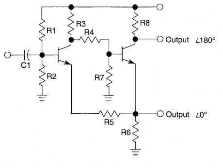
This sine-wave triggered circuit produces two square-wave outputs that are 180° out of phase. (View)
View full Circuit Diagram | Comments | Reading(2358)
A_D_CONVERTER_FOR_PCs
Published:2009/6/18 22:57:00 Author:May
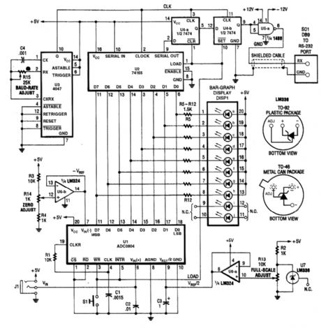
An ADC0804 A/D converter converts analog data to digital. This is fed ister and converted to serial data. U3 provides a baud-rate clock. U4A and start and stop bits needed at beginning and end of each data word. (View)
View full Circuit Diagram | Comments | Reading(3452)
HIGH_SPEED_A_D_CONVERTER_SYSTEM
Published:2009/6/18 22:54:00 Author:May
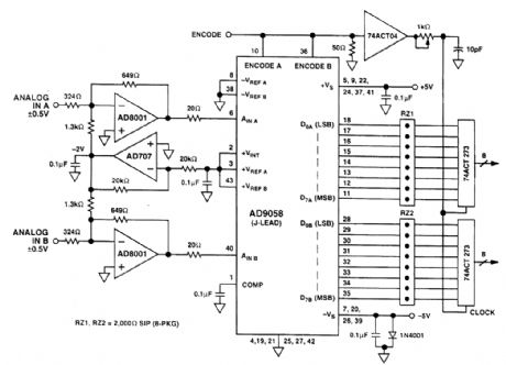
The AD8001 is well suited for driving high-speed analog-to-digital converters, such as the AD9058.The AD9058 is a dual 8-bit 50 Msps ADC. In the circuit shown, there are two AD8001s driving the in-puts of the AD905f8 which are configured for 0- to +2-V ranges. Bipolar input signals are buffered, amplified (-2x), and offset (by +1.0 V) into the proper input range of the ADC. Using the AD9058's internal +2-V reference connected to both ADCs (as shown) reduces the number of external com-ponents required to create a complete data acquisition system. The 20-Ω resistors in series with ADC input are used to help the AD8001 drive the 10-pf' ADO input capacitance. The two AD8001s only add 100 mW to the power consumption while not limiting the performance of the circuit. (View)
View full Circuit Diagram | Comments | Reading(1017)
dc_to_dc_CONVERTER_II
Published:2009/6/18 2:40:00 Author:May
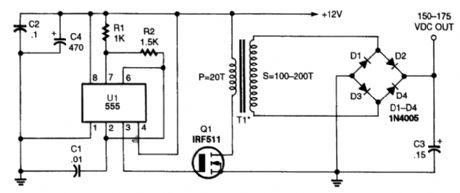


In this dc-to-dc converter, the 555 is used to produce a rising and collapsing field in TI's primary, generating a high voltage in TI's secondary winding. That voltage is then full-wave, bridge rectified by Dl through D4, and filtered by C3. T1 is an Amidon Associates EA-775-375E core and nylon bob-bin, with #26 wire for the primary and #28 or #30 for the secondary. About 5 W of power is available. (View)
View full Circuit Diagram | Comments | Reading(3887)
NEGATIVE_STEP_up_dc_to_dc_CONVERTER
Published:2009/6/18 2:37:00 Author:May
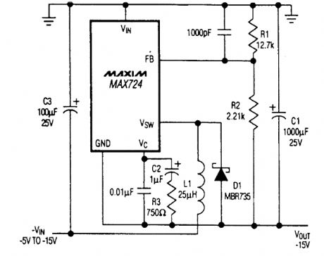
A Maxim MAX724 is used in a step-up switching converter to provide -15-V output from a-5-to-15-V input. (View)
View full Circuit Diagram | Comments | Reading(974)
ULTRA_LOW_POWER_dc_to_dc_CONVERTER_FOR_PERSONAL_COMMUNICATIONS_PRODUCTS
Published:2009/6/18 2:30:00 Author:May


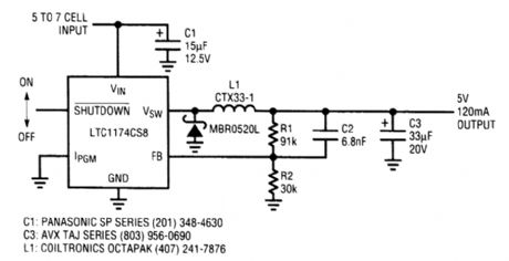
The LTC1174 step-down converter is designed specifically to eliminate noise at audio frequen-cies while maintaining high efficiency at low output currents. This circuit shows a 5-V, 120-mA out-put derived from 5 to 7 NiCad or NiMH cells. Small input and output capacitors that are capable of handling the necessary ripple currents help conserve space. In applications where shutdown is de-sired, this feature is available (otherwise short this pin to Vin).The LTC1174's internal switch, connected between Vin and Vsw is current controlled at a peak of approximately 340 mA. Low peak switch current is one of the key features that allows the LTC1174 to minimize system noise compared to other chips that carry significantly higher peak currents, eas-ing shielding and filtering requirements, and decreasing component stresses. Output current of up to 450 mA is possible with this device by connecting the 1 pgm pin to Vin. This increases the peak current to 600 mA, allowing for a high average output current. (View)
View full Circuit Diagram | Comments | Reading(872)
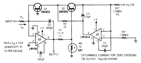
VOLTAGE_CONTROLLED_CURRENT_SINK
Published:2009/6/18 2:17:00 Author:May

A voltage-variable current sink is shown in the figure. The output current is 1 mA per volt of Vin(as R5 = 1 kΩ and the gain is +1). This circuit provides approximately 0 mA output current for Vin = 0 V DCL. (View)
View full Circuit Diagram | Comments | Reading(1)
dc_dc_CONVERTER_CIRCUIT_WITH_33_V_AND_5_V_OUTPUTS
Published:2009/6/17 4:35:00 Author:May
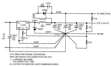
Input voltages can range from 8 V to 30 V. The load range on the 5 V is 0.05 A to 5 A while the 3.3-V load range is 0.1 A to I A. The circuit is self-protected under no-load conditions. Over all load and line conditions, including cross regulation, the 3.3-V output varies from 3.25 V to 3.27 V. The 5-V output varies from 4.81 Y to 5.19 V under the same conditions.In a typical application to 0.5 A on the 3.3 V and 0.25 A on the 5 V, efficiency is typically 76%. With an input voltage of 30 V and a full-load condition, the efficiency drops to 66%. In normal oper-ating regions, efficiency is always better than 70%. The 5-V ripple is less than 75 mV and the 3.3-V ripple less than 50 mV over all line and load conditions. (View)
View full Circuit Diagram | Comments | Reading(956)
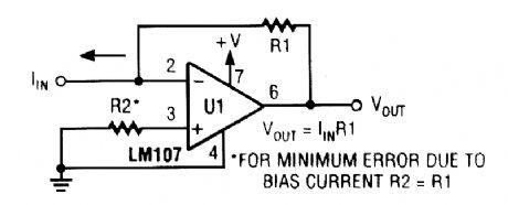
TEMPERATURE_COMPENSATED_ONE_QUADRANT_LOGARITHMIC_CONVERTER
Published:2009/6/17 4:33:00 Author:May
A logarithmic converter used to produce an output voltage that is proportional to the logarithm of an input current is shown. RS is the input impedance of the input source. (View)
View full Circuit Diagram | Comments | Reading(675)
CURRENT_TO_VOLTAGE_CONVERTER
Published:2009/6/17 4:30:00 Author:May
View full Circuit Diagram | Comments | Reading(5)
28_Vdc_TO_5_Vdc_CONVERTER
Published:2009/6/17 4:30:00 Author:May
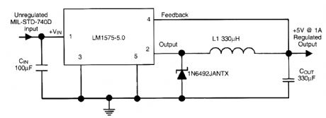
The National Semiconductor LM1575-5.0 allows a very simple switching regulator, with >80% ef-ficiency; operating as a 5-V source @ 1A from a +28-V bus. (View)
View full Circuit Diagram | Comments | Reading(1040)
ATV_DOWNCONVERTER
Published:2009/6/17 4:28:00 Author:May
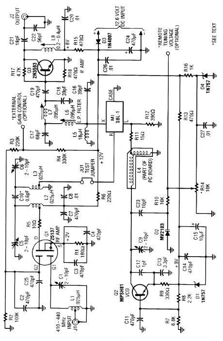
This RF converts amateur TV signals in the 420- to 450-MHz region to VHF channel 3 or 4, allowing reception of those signals on a standard TV receiver. RF amplifier Q1 feeds mixer M1, and Q3 acts as an IF amplifier. Q2 is an oscillator operating around 378 MHZ and is tuneable over about a 30-MHz range. A complete kit is available from North Country Radio, P.O. Box 53, Wykagyl Station, NY 10804 (View)
View full Circuit Diagram | Comments | Reading(1214)
SINE_WAVE_TO_SQUARE_WAVE_CONVERTER
Published:2009/6/17 4:19:00 Author:May
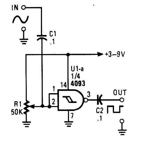
This circuit tums a sine wave into a square wave. It is comprised of a single 2-input NAND Schmitt trigger that's conftgured as an inverter with a trigger level adjustment at its input. As the input voltage rises above the gate's trigger point, the output snaps to its alternate state, producing a square-wave output. (View)
View full Circuit Diagram | Comments | Reading(2886)
SINE_TO_SQUARE_WAVE_CONVERTER
Published:2009/6/17 4:15:00 Author:May
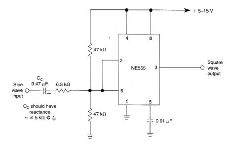
This 555-based Schmitt trigger circuit is useful for creating clock pulses from analog signals since it readily converts sine waves into square waves. (View)
View full Circuit Diagram | Comments | Reading(4503)
SIMPLE_2_m-6_m_TRANSVERTER
Published:2009/6/17 4:14:00 Author:May
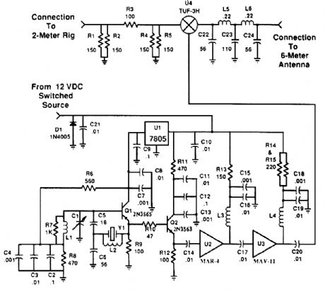
Using the bilateral properties of a balanced mixer this transverter will produce 6-m output with 2-m inputs. Y1 is a 90-MHz crystal. Note that the input on 2 m is 143 to 144 MHz for 53 to 54-MHz output. This avoids possibility of extraneous 2-m reception during receive periods. If your radio will not transmit below 144 MHz, then use a 93- or 94-MHz crystal frequency. (View)
View full Circuit Diagram | Comments | Reading(1629)
TEMPERATURE_TO_DIGITAL_CONVERTER
Published:2009/6/17 4:12:00 Author:May
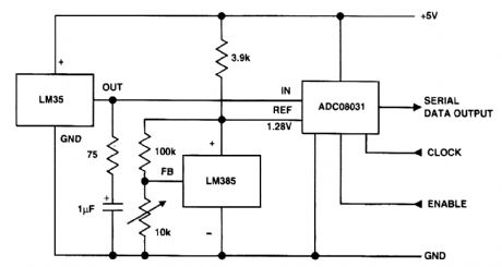
The devices shown from National Semiconductor are used in digital temperature circuit sensor LM35 and reference LM385 feed A-D converter ADC08031. (View)
View full Circuit Diagram | Comments | Reading(2750)
CRYSTAL_CONTROLLED_FREQUENCY_CONVERTER_USING_MOSFET
Published:2009/6/17 4:11:00 Author:May
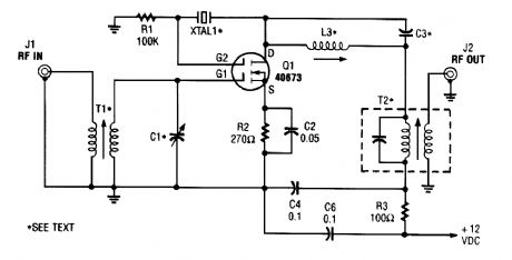
The second gate (G2) of a MOSFET can be used to incorporate a crystal oscillator into the same stage as a frequency mixer. Although old hat with tubes, this scheme is seldom seen in dual-gate MOSFET circuitry. L3, C3, and XI form the crystal oscillator, and T2 is an IF output transformer. T1 and C1 are tuned to the converter input frequency. This circuit should be useable up to 25 MHz or so, or higher with third-overtone crystals. (View)
View full Circuit Diagram | Comments | Reading(3125)
800_TO_1000_MHz_SCANNER_CONVERTER
Published:2009/6/17 4:09:00 Author:May
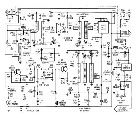
This converter enables reception of 800 to 1000 MHz on any scanner covering the 400 to 500-MHz range. The converter can be set up to cover either 800 to 900 MHz or by readjustment 900 to 1000 MHz. Sensitivity is very high because of the GASFET front end. For best results, the scanner should be of a programmable variety. A complete kit is available from North Country Radio, P.O. Box 53, Wykagyl Station, NY 10804. (View)
View full Circuit Diagram | Comments | Reading(1133)
VLF_CONVERTER
Published:2009/6/17 4:05:00 Author:May

This converter converts10 kHz to 150 kHz to 4.01 to 4.15 MHz for use with a shortwave receiver for VLF reception. A 4-MHz L.O. frequency is used. X1 can be a microprocessor XTAL or another suitable type. The antenna should be as long as possible. (View)
View full Circuit Diagram | Comments | Reading(1)
TEMPERATURE_TO_FREQUENCY_CONVERTER
Published:2009/6/17 4:03:00 Author:May
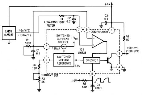
In this circuit an LM34 or LM35 produces a frequency proportional to temperature. Reference current (138 μA) is set via R3. The output can be used to drive a display, frequency counter, or other indicating device for temperature readout. (View)
View full Circuit Diagram | Comments | Reading(0)
| Pages:22/24 At 2021222324 |
Circuit Categories
power supply circuit
Amplifier Circuit
Basic Circuit
LED and Light Circuit
Sensor Circuit
Signal Processing
Electrical Equipment Circuit
Control Circuit
Remote Control Circuit
A/D-D/A Converter Circuit
Audio Circuit
Measuring and Test Circuit
Communication Circuit
Computer-Related Circuit
555 Circuit
Automotive Circuit
Repairing Circuit