
Index 247
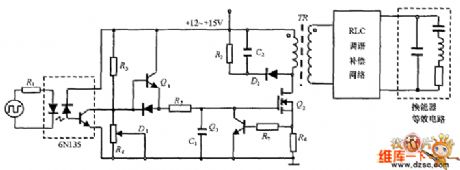
Ultrasonic transducer drive circuit diagram
Published:2011/3/28 1:54:00 Author:Nicole | Keyword: ultrasonic transducer drive
View full Circuit Diagram | Comments | Reading(4250)
Electromagnet drive circuit diagram
Published:2011/3/28 1:49:00 Author:Nicole | Keyword: Electromagnet drive

View full Circuit Diagram | Comments | Reading(793)
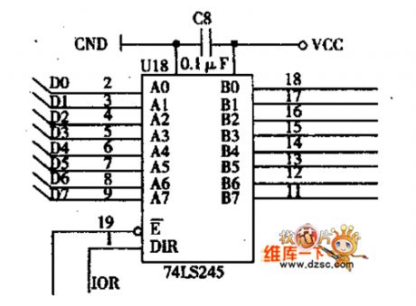
Data buffer and drive circuit diagram
Published:2011/3/28 1:47:00 Author:Nicole | Keyword: data buffer, drive
View full Circuit Diagram | Comments | Reading(565)
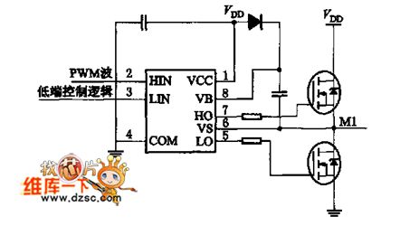
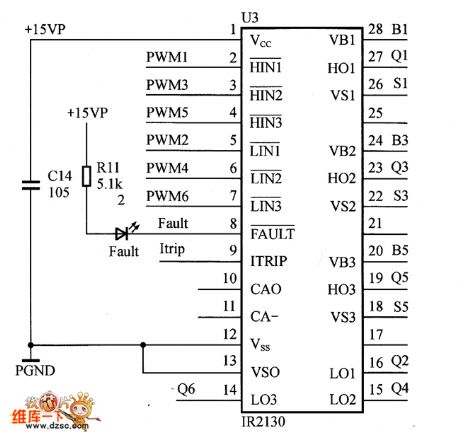
Drive circuit diagram with IR2103
Published:2011/3/27 20:08:00 Author:Nicole | Keyword: drive
View full Circuit Diagram | Comments | Reading(5212)
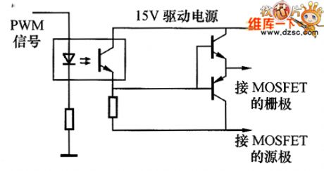
Output drive circuit diagram with photoelectric isolation
Published:2011/3/27 20:07:00 Author:Nicole | Keyword: Output drive
View full Circuit Diagram | Comments | Reading(643)
No external delay circuit diagram
Published:2011/3/25 2:30:00 Author:Rebekka | Keyword: No external delay
No external delay circuit diagram is shown as below.
(View)
View full Circuit Diagram | Comments | Reading(481)
External delay circuit diagram
Published:2011/3/25 2:32:00 Author:Rebekka | Keyword: External delay
External delay circuit diagram is shown as below.
(View)
View full Circuit Diagram | Comments | Reading(536)
Boost PWM circuit diagram
Published:2011/3/28 1:18:00 Author:Rebekka | Keyword: Boost PWM
Boost PWM circuit diagram is shown as below.
(View)
View full Circuit Diagram | Comments | Reading(973)
Driver Interface circuit diagram
Published:2011/3/25 1:18:00 Author:Rebekka | Keyword: Driver Interface
Driver Interface circuit diagram is shown as below.
(View)
View full Circuit Diagram | Comments | Reading(530)
Three-phase full-bridge circuit diagram
Published:2011/3/28 1:26:00 Author:Rebekka | Keyword: Three-phase full-bridge
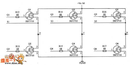
Three-phase full-bridge circuit diagram is shown as below.
(View)
View full Circuit Diagram | Comments | Reading(652)
Current detection part circuit diagram
Published:2011/3/28 1:25:00 Author:Rebekka | Keyword: Current detection part
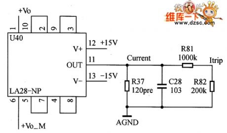
Current detection part circuit diagram is shown as below.
(View)
View full Circuit Diagram | Comments | Reading(486)
Over-current protection circuit diagram
Published:2011/3/28 1:23:00 Author:Rebekka | Keyword: Over-current protection
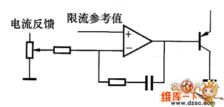
Over-current protection circuit diagram is shown as below.
(View)
View full Circuit Diagram | Comments | Reading(598)
Boost chopper circuit overvoltage protection circuit diagram
Published:2011/3/28 1:22:00 Author:Rebekka | Keyword: Boost chopper, overvoltage protection
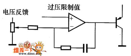
Boost chopper circuit overvoltage protection circuit diagram is shown as below.
(View)
View full Circuit Diagram | Comments | Reading(747)
Buck Chopper driving circuit diagram
Published:2011/3/28 1:20:00 Author:Rebekka | Keyword: Buck Chopper
Buck Chopper driving circuit diagram is shown as below.
(View)
View full Circuit Diagram | Comments | Reading(789)
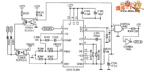
TL494 PWM circuit diagram
Published:2011/3/29 4:05:00 Author:Rebekka | Keyword: PWM
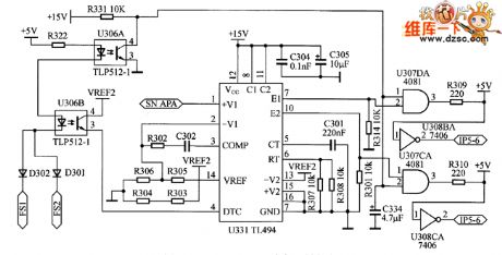
TL494 PWM circuit diagram is shown as below. The pin 5 and 6 of chip connect to resistor R301 and capacitor C301. It makes sure TL494 oscillator frequency sawtooth is: f=1.1/(RTCT)=25KHz.
(View)
View full Circuit Diagram | Comments | Reading(10621)
MFBP Delay equalizer circuit diagram
Published:2011/3/25 1:27:00 Author:Rebekka | Keyword: Delay equalizer, MFBP
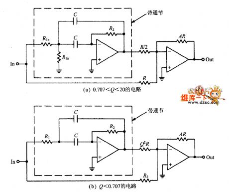
MFBP Delay equalizer circuit diagram is shown as below.
(View)
View full Circuit Diagram | Comments | Reading(700)
DABP Delay equalizer circuit diagram
Published:2011/3/25 1:28:00 Author:Rebekka | Keyword: Delay equalizer, DABP
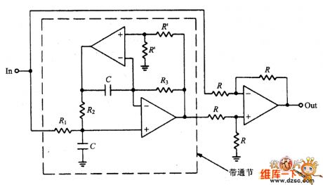
DABP Delay equalizer circuit diagram is shown as below.
(View)
View full Circuit Diagram | Comments | Reading(715)
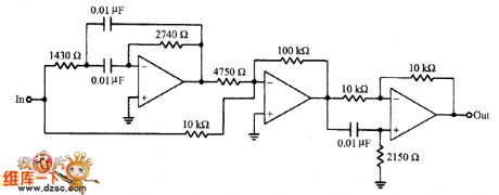
Network delay time-domain circuit diagram
Published:2011/3/29 4:00:00 Author:Rebekka | Keyword: Network delay time-domain
Network delay time-domain circuit diagram is shown as below.
(View)
View full Circuit Diagram | Comments | Reading(425)
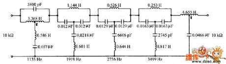
100μs delay line circuit diagram
Published:2011/3/29 3:57:00 Author:Rebekka | Keyword: 100μs delay line
100μs delay line circuit diagramis shown as below.
(View)
View full Circuit Diagram | Comments | Reading(1405)
Current mirror-based current-controlled drive circuit diagram
Published:2011/3/28 2:25:00 Author:Rebekka | Keyword: Current mirror-based, current-controlled drive

Current mirror-based current-controlled drive circuit diagram is shown as below.
(View)
View full Circuit Diagram | Comments | Reading(528)
| Pages:247/250 At 20241242243244245246247248249250 |
Circuit Categories
power supply circuit
Amplifier Circuit
Basic Circuit
LED and Light Circuit
Sensor Circuit
Signal Processing
Electrical Equipment Circuit
Control Circuit
Remote Control Circuit
A/D-D/A Converter Circuit
Audio Circuit
Measuring and Test Circuit
Communication Circuit
Computer-Related Circuit
555 Circuit
Automotive Circuit
Repairing Circuit