
Index 448
74 series digital circuit of 7497 synchronous 6 binary coefficient multiplier
Published:2011/4/2 3:58:00 Author:Ecco | Keyword: digital circuit , synchronous 6 , binary coefficient, multiplier
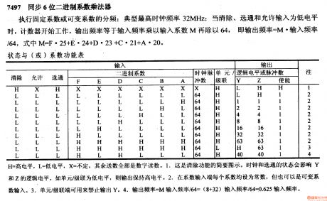
Executive fixed coefficient or variable coefficient fractional frequency: typical highest clock frequency 32MHz; When clearing, choose input for low level, counter begins the work, the output frequency equals to input frequency multiplied by input coefficient divided by 64.
H is high level, L is low level, X is uncertain, others are digital reading. 1. This is a simple chart to show the clearing function. The state of clock and strobe will make an influence on the logic level of Y and Z. For example, the unit /cascade is in low level, the output will keep high level. 2. The coefficient in input terminal is constant or variable coefficient input. 3. The unit/cascade is not allow to output Y. (View)
View full Circuit Diagram | Comments | Reading(728)
74 series digital circuit of 74H62 4 input AND-OR expander
Published:2011/4/5 22:49:00 Author:Ecco | Keyword: digital circuit, 4 input , expander
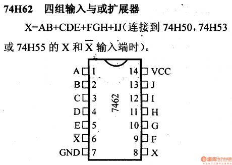
74H62 4 input AND-OR expander
X=AB+CDE+FGH+IJ(when connecting to the X input terminal of 74H50, 74H53 or 74H55)
(View)
View full Circuit Diagram | Comments | Reading(588)
74 series digital circuit of 74LS63 hex current-reading interface gate
Published:2011/4/5 22:48:00 Author:Ecco | Keyword: digital circuit, hex current-reading, interface gate
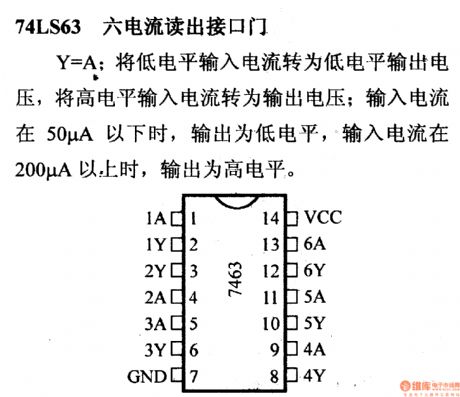
74LS63 hex current-reading interface gate
Y=A; The input current in low level becomes output voltage, the input current in high level becomes output voltage; The input current is lower than 50μA, the output is in low level, the input current is higher than 200μA, the output is in high level. (View)
View full Circuit Diagram | Comments | Reading(700)
The series input voltage feedback
Published:2011/4/14 2:28:00 Author:Ecco | Keyword: series input , voltage feedback
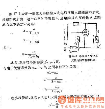
The figure 17-1 shows the basic form of the first-stage amplifier series input voltage feedback circuit.
(View)
View full Circuit Diagram | Comments | Reading(518)
Digital counter demonstration circuit
Published:2011/4/12 22:01:00 Author:Nicole | Keyword: digital counter
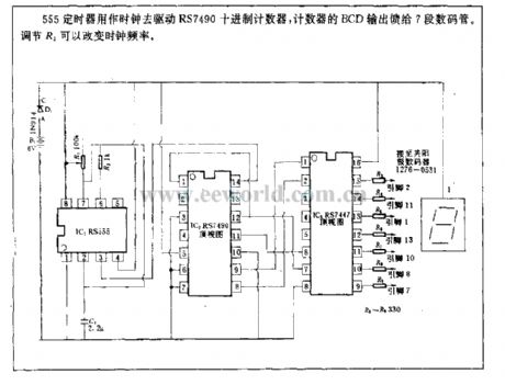
555 timer is used as clock to drive RS7490 decimal timer, BCD output to 7 section LED. To adjust R1 can change the clock frequency. (View)
View full Circuit Diagram | Comments | Reading(2802)
Shunt regulator circuit
Published:2011/3/30 22:06:00 Author:may | Keyword: Shunt regulator
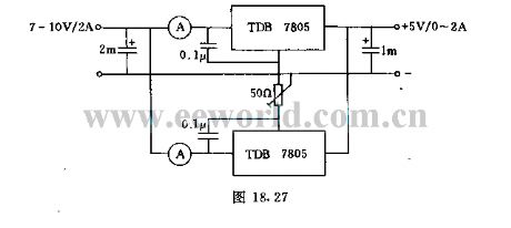
This circuit use two intergrated regulator 7058 parallel connection, every voltage regulator circuit input side all switch-in 0.1µF capacitor to clear high frequency oscillation. (View)
View full Circuit Diagram | Comments | Reading(701)
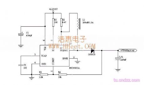
2.2~6V output 7V voltage booster circuit
Published:2011/4/1 22:27:00 Author:may | Keyword: 2.2~6V, output 7V, voltage booster
View full Circuit Diagram | Comments | Reading(702)
Three time base window circuit
Published:2011/3/31 22:37:00 Author:may | Keyword: time base window
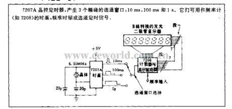
7207A crystal controlled timer, generate three precise gating window: 10ms, 100ms and 1s. They can use as time base of cymometer ( such as 7208) , sanction time scale or gating timmer signal.
(View)
View full Circuit Diagram | Comments | Reading(444)
3 integrated voltage stabilizer parallel expansion output current
Published:2011/3/31 21:24:00 Author:may | Keyword: integrated voltage stabilizer, parallel expansion
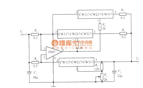
View full Circuit Diagram | Comments | Reading(502)
1024 bit CCPD support drive circuit
Published:2011/4/2 1:03:00 Author:may | Keyword: 1024 bit, support drive
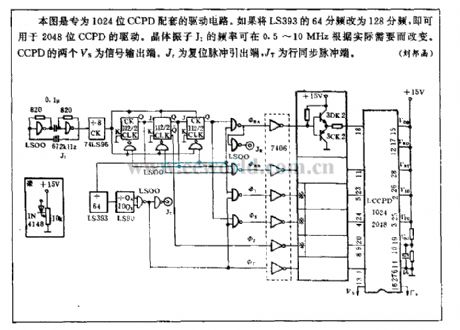
The diagram is drive circuit which is support to 1024 bit CCPD. It can used for drive of 1024 bit CCPD if change 64 frequency division of LS393 to 128 frequency division. The frequency of quartz crystal unit J1 can change according to actual need at the range of 0.5~10MHz. Two Vs of CCPD is signal output end. Jr is reset pulse exit side. JT is line synchronizing pulse side.
(Liu banghan)
(View)
View full Circuit Diagram | Comments | Reading(436)
1,024 bits CCD drive circuit
Published:2011/3/21 0:38:00 Author:muriel | Keyword: 1,024 bits, CCD drive circuit
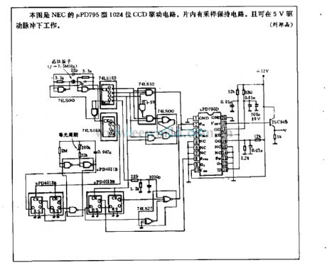
This figure is NEC's uPD795 type 1024bits CCD drive circuit,In the chip hassample hold circuit. And can work at 5V drive pulse. (View)
View full Circuit Diagram | Comments | Reading(1227)
12 or 24h clock circuit
Published:2011/4/2 1:40:00 Author:may | Keyword: 12 or 24h, clock
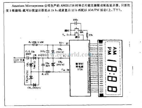
AMIS1736 clock chip is produced by American Microsystems company. It can drive LCD directly. The display equipment can display 24h or display 12h coupled with AM/PM mark (Mornings And Afternoons) if only we we change three connections.
(View)
View full Circuit Diagram | Comments | Reading(2229)
UPS-500W circuit diagram 2
Published:2011/4/14 3:44:00 Author:Nicole | Keyword: UPS-500W
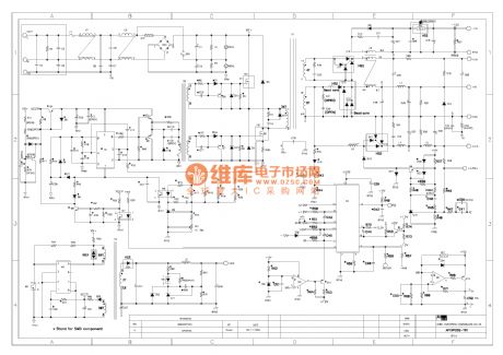
View full Circuit Diagram | Comments | Reading(5845)
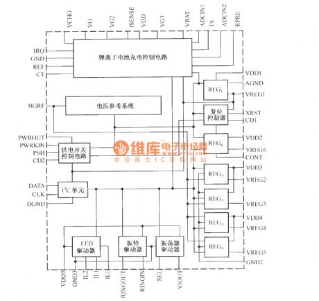
TWL2213 internal structure block diagram
Published:2011/4/14 4:01:00 Author:Nicole | Keyword: internal structure
View full Circuit Diagram | Comments | Reading(487)
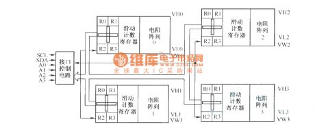
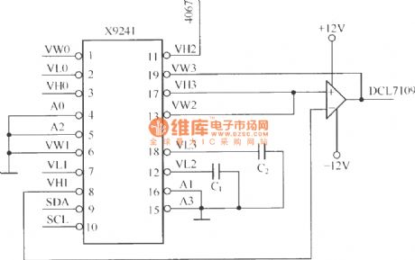
X9241 functional block diagram and application
Published:2011/4/14 4:16:00 Author:Nicole | Keyword: functional block diagram
View full Circuit Diagram | Comments | Reading(750)
IGBTNPT structural main parasitic component and equivalent circuit
Published:2011/4/13 3:26:00 Author:Nicole | Keyword: IGBTNPT, parasitic component
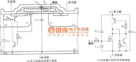
View full Circuit Diagram | Comments | Reading(501)
MIC79050-4.2BS internal structure block diagram
Published:2011/4/13 3:30:00 Author:Nicole | Keyword: internal structure

MIC79050-4.2BS is a precise LDO linear regulated power supply, the output voltage is 4.2V. (View)
View full Circuit Diagram | Comments | Reading(644)
Adjustable constant flow source with BG602
Published:2011/3/30 2:21:00 Author:muriel | Keyword: adjustable , constant flow source
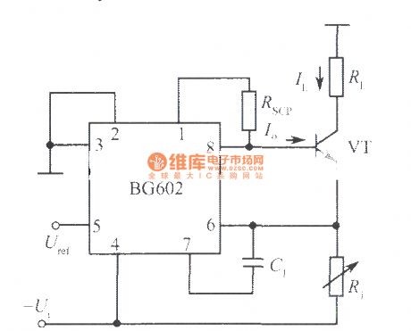
View full Circuit Diagram | Comments | Reading(454)
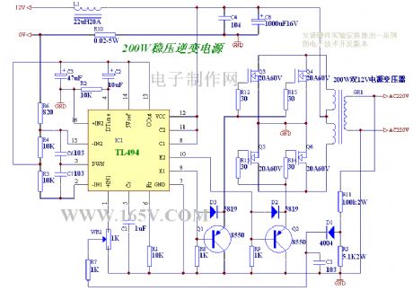
Inverter circuit 9
Published:2011/4/13 21:53:00 Author:may | Keyword: Inverter
View full Circuit Diagram | Comments | Reading(1101)
Inverter circuit 8
Published:2011/4/13 21:51:00 Author:may | Keyword: Inverter
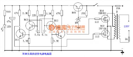
simple and practical inverter power supply circuit (View)
View full Circuit Diagram | Comments | Reading(1211)
| Pages:448/471 At 20441442443444445446447448449450451452453454455456457458459460Under 20 |
Circuit Categories
power supply circuit
Amplifier Circuit
Basic Circuit
LED and Light Circuit
Sensor Circuit
Signal Processing
Electrical Equipment Circuit
Control Circuit
Remote Control Circuit
A/D-D/A Converter Circuit
Audio Circuit
Measuring and Test Circuit
Communication Circuit
Computer-Related Circuit
555 Circuit
Automotive Circuit
Repairing Circuit