
Index 453
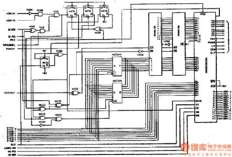
Synchronous access mode realization circuit diagram of liquid crystal display
Published:2011/4/7 21:47:00 Author:Ecco | Keyword: Synchronous access mode, liquid crystal display
View full Circuit Diagram | Comments | Reading(533)
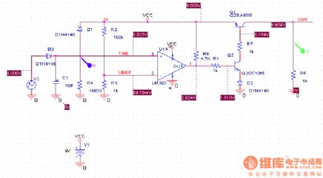
Multimeter delay switch circuit diagram
Published:2011/4/7 3:06:00 Author:Ecco | Keyword: Multimeter , delay switch
View full Circuit Diagram | Comments | Reading(597)
The push-pull circuit diagram without output transformer
Published:2011/4/8 1:40:00 Author:Ecco | Keyword: push-pull circuit , without output transformer
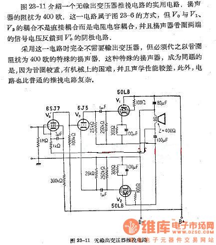
Figure 28-11 describes a practical circuit of push-pull circuit without output transformer. The impedance of speakers is 400Ω. The circuit is using the way of Figure 23-6, but the coupling between V0 and V1, V2 is not directly coupled but the coupling of the resistance and capacitance, and the signal voltage of loudspeaker is feedbacked to the cathode circuit of V0. The circuit doesn't need output transformer, but replaced by a special speaker with voice coil impedance in 400Ω. As the voice coil that is relatively heavy, so the problem is that there are mechanical difficulties, and the acoustic performance is poor, in addition, the push-pull circuit more complex than the normal.
(View)
View full Circuit Diagram | Comments | Reading(679)
The basic form circuit diagram of serial input current feedback
Published:2011/4/8 2:01:00 Author:Ecco | Keyword: basic form , serial input, voltage feedback
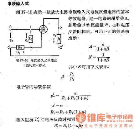
Figure 17-10 shows a basic equivalent circuit of serial input current feedback circuit in an amplifier circuit. The net gain of this circuit a, the total amount of gain A and feedback N, are the same with voltage feedback.
(View)
View full Circuit Diagram | Comments | Reading(529)
The basic form 2 of parallel input voltage feedback
Published:2011/4/8 1:55:00 Author:Ecco | Keyword: basic form , parallel input , voltage feedback
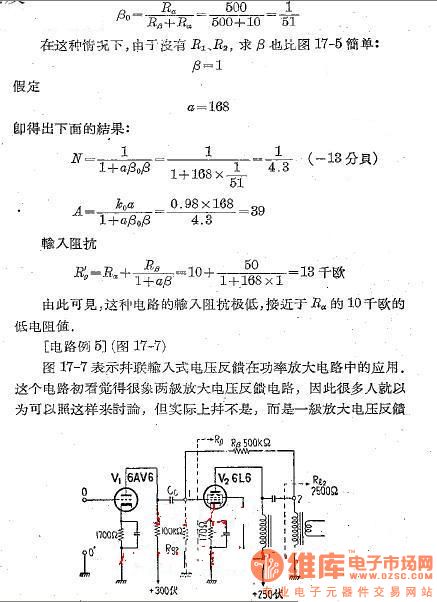
Figure 17-7 shows the applications of parallel input voltage feedback in power amplifier circuit.At first glance this circuit is like poles amplification voltage feedback circuit, so many people think they can be discussed according to this, but actually it's wrong, this is a pole amplification voltage feedback.
(View)
View full Circuit Diagram | Comments | Reading(459)
The basic form 1 of parallel input voltage feedback
Published:2011/4/8 1:46:00 Author:Ecco | Keyword: basic form, parallel input , voltage feedback
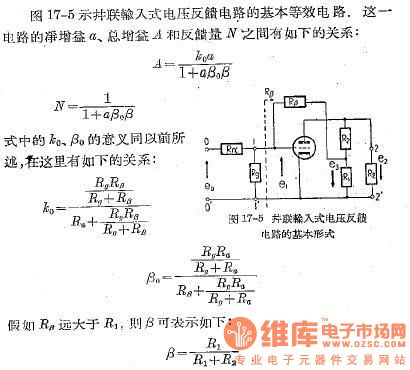
Figure 17-5 shows the the basic equivalent circuit of parallel input voltage feedback circuit.
(View)
View full Circuit Diagram | Comments | Reading(527)
The display application circuit diagram of 74LS161 counter
Published:2011/4/8 2:12:00 Author:Ecco | Keyword: display application , counter
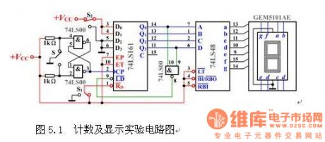
The display application circuit diagram of counter is as the chart 5.1
(View)
View full Circuit Diagram | Comments | Reading(4824)
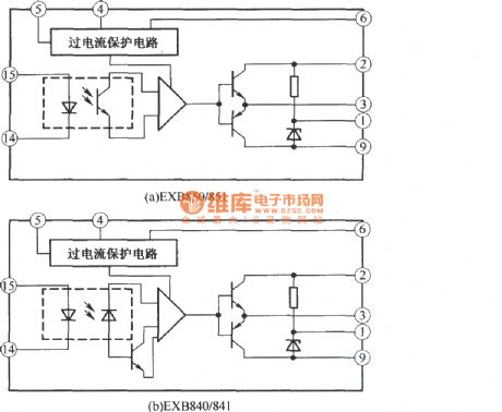
The function block diagram of EXB series driver
Published:2011/4/8 2:25:00 Author:may | Keyword: driver
View full Circuit Diagram | Comments | Reading(660)
Short-circuit protection function test method 1 of IGBT drive circuit
Published:2011/4/8 1:29:00 Author:may | Keyword: Short-circuit protection, function test method, IGBT drive
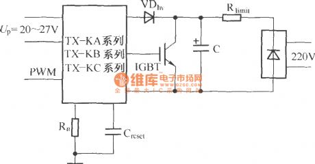
The main problem IGBT solved is how to better protecting IGBT under the situation of over current, short circuit and over voltage. The error of over current generally need longer time to make the power supply to over heating, so the protection to it is mainly solve by main control board. In the diagram, C=10~470μF,Rlimit=10~100Ω,Creset =10nF. (View)
View full Circuit Diagram | Comments | Reading(2139)
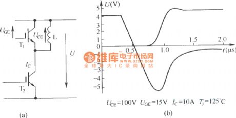
IGBT switch equivalent circuit and open wave form
Published:2011/4/8 1:19:00 Author:may | Keyword: IGBT switch, equivalent, open wave form
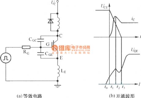
(a) equivalent circuit(b) open wave form (View)
View full Circuit Diagram | Comments | Reading(2013)
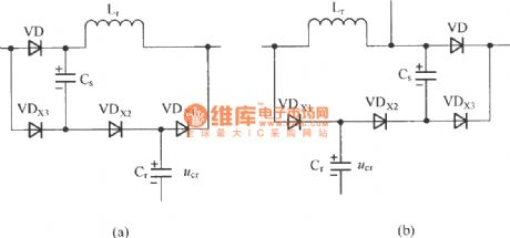
Reduced series resonant inverter main topological structure with resonance pole capacitor buffer
Published:2011/4/7 4:41:00 Author:may | Keyword: series resonant inverter, topological structure, resonance pole, capacitor buffer
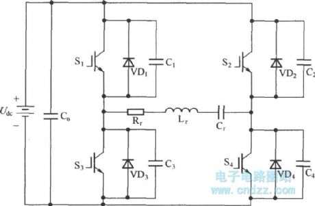
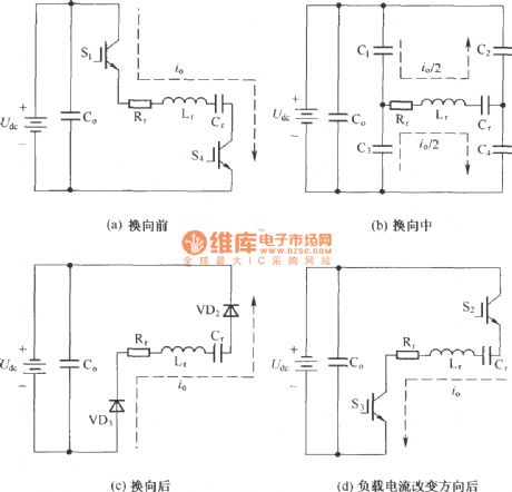
Series resonant inverter with resonance pole capacitor buffer’s process of changing current:
Routine RCVD buffer circuit adopts resistor to discharge, with the increase of switch frequency, the power consume in buffer is increase too, greatly reduce the efficiency of the whole inverter system. It can effectively reduce the shutoff loss of switch device that directly parallel connect a non-loss buffer capacitor between IGBT collector and emitter. It is more fit for high frequency inverter to feedback the power of the resistor loss in routine buffer to load or power supply.
(View)
View full Circuit Diagram | Comments | Reading(3555)
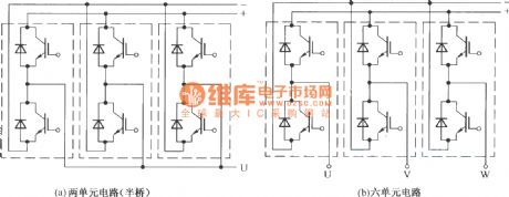
Single-phase topological structure of cascade connection multilevel inverter basing on star point clamp type
Published:2011/4/7 4:23:00 Author:may | Keyword: Single-phase topological structure, cascade connection, multilevel inverter, star point clamp type
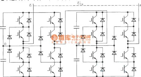
View full Circuit Diagram | Comments | Reading(2224)
IGBT shut off voltage wave and chopper circuit in advanced hard switching chopper circuit
Published:2011/4/7 4:05:00 Author:may | Keyword: IGBT shut off voltage wave, chopper, hard switching chopper
View full Circuit Diagram | Comments | Reading(870)
The circuit and shutoff wave in two reverse blocking type IGBT reverse parallel connection
Published:2011/4/7 4:05:00 Author:may | Keyword: reverse blocking type, IGBT, reverse parallel connection, shutoff wave
View full Circuit Diagram | Comments | Reading(573)
Passive Lossless cushion circuit topological structure
Published:2011/4/6 4:22:00 Author:may | Keyword: passive Lossless, cushion, topological structure
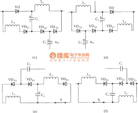
Passive Lossless cushion circuit topological structure include two classes:1, minimum voltage stress element (MVS), is shown in diagram (a), (b)2 non-minimum voltage stress element (Non-MVS) , is shown in diagram (c), (d), (e), (f)
(View)
View full Circuit Diagram | Comments | Reading(620)
SKiiPPACK element circuit
Published:2011/4/6 3:36:00 Author:may | Keyword: element
SKiiPPACK(Swmikron Integrated Intelligent Power Pack) series module is different from traditionary IGBT module. In SKiPPACK, DCB uropatagia with IGBT and diode chip is not weld at on one copper base, but get help from pressure unit of composite material, press almost the whole on radiator. (View)
View full Circuit Diagram | Comments | Reading(676)
Output stage of SKHI series driver
Published:2011/4/6 3:30:00 Author:may | Keyword: Output stage, driver
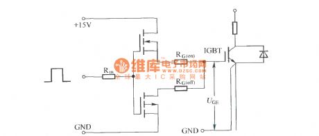
SKHI series driver divide RG into RG(on) and RG(off), shown above. This two parameters can control separately, and can separately adjust RG(on) and RG(oof) according to the capacity of IGBT, in order to get best drive effects. (View)
View full Circuit Diagram | Comments | Reading(520)
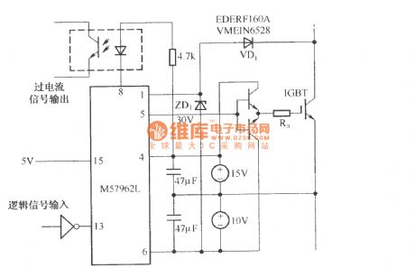
M57962L driving high power IGBT module typical circuit
Published:2011/4/6 5:07:00 Author:may | Keyword: high power IGBT module
View full Circuit Diagram | Comments | Reading(2922)
M57962L internal structure block diagram
Published:2011/4/6 3:06:00 Author:may | Keyword: internal structure
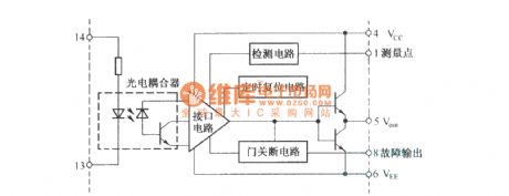
View full Circuit Diagram | Comments | Reading(669)
N groove IGBT simplify equivalent circuit and electric graphic symbol
Published:2011/4/6 4:56:00 Author:may | Keyword: N groove IGBT, simplify equivalent, electric graphic symbol
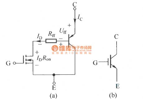
View full Circuit Diagram | Comments | Reading(724)
| Pages:453/471 At 20441442443444445446447448449450451452453454455456457458459460Under 20 |
Circuit Categories
power supply circuit
Amplifier Circuit
Basic Circuit
LED and Light Circuit
Sensor Circuit
Signal Processing
Electrical Equipment Circuit
Control Circuit
Remote Control Circuit
A/D-D/A Converter Circuit
Audio Circuit
Measuring and Test Circuit
Communication Circuit
Computer-Related Circuit
555 Circuit
Automotive Circuit
Repairing Circuit