
Computer-Related Circuit
Index 21
Eight_channel_data_acquisition_circuit_for_the_M6800
Published:2009/7/21 8:32:00 Author:Jessie
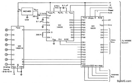
Eight-channel data acquisition circuit for the M6800 (courtesy Motorola Semiconductor Products Inc.). (View)
View full Circuit Diagram | Comments | Reading(1508)
Memory_core_sense_amplifier_using_an_MC1514
Published:2009/7/21 8:30:00 Author:Jessie
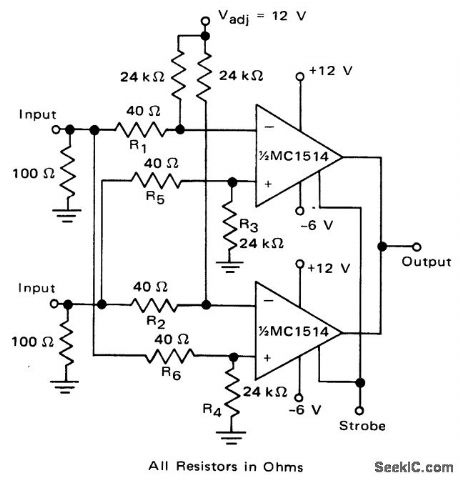
Memory core sense amplifier using an MC1514 (courtesy Motorola Semiconductor Products Inc.). (View)
View full Circuit Diagram | Comments | Reading(870)
Sequentially_addressed_8_channel_data_acquisition_subsystem_capable_of_acquiring_data_to_12_bit_accuracy_at_a_220_kHz_throughput_rate
Published:2009/7/21 8:29:00 Author:Jessie
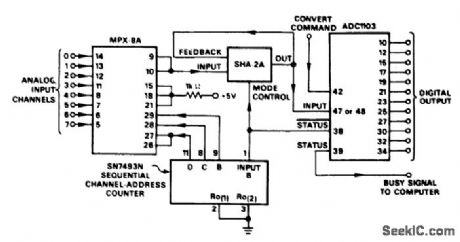
Sequentially addressed 8-channel data acquisition subsystem capable of acquiring data to 12-bit accuracy at a 220 kHz throughput rate. The MPX-8A is a multiplexor, the SHA-2A a sample-and-hold amplifier and the ADC1103 a high-speed A/D converter (courtesy Analog Devices, Inc.). (View)
View full Circuit Diagram | Comments | Reading(885)
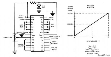
Output_storage_register_using_an_ADC171_dual_slope_integrating_A_D_converter
Published:2009/7/21 8:25:00 Author:Jessie
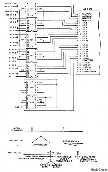
Output storage register using an ADC171 dual-slope integrating A/D converter (courtesy Analog Devices, Inc.). (View)
View full Circuit Diagram | Comments | Reading(849)
DATA_SEPARATOR_FOR_FLOPPY_DISKS
Published:2009/6/30 23:42:00 Author:May
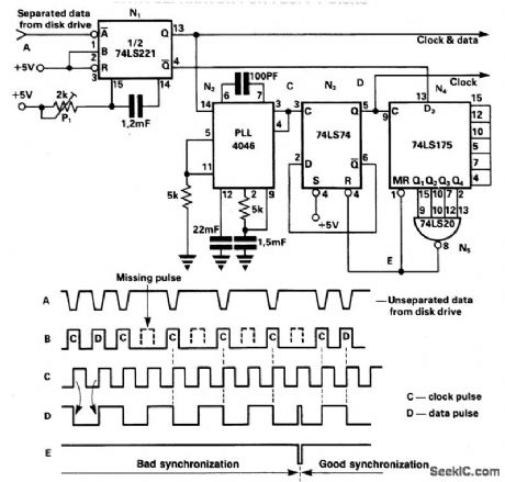
The data separator is intended for use with 8 flexible diskettes with IBM 3870 soft sectored format. The circuit delivers data and clock (B) and clock pulses (D). These two signals must be in such a sequence that the negative edge of the clock pulse is at the middle of a data cell.Unseparated data (A) from the floppy unit is shaped with one shot N1. Trimmer P1 should be adjusted so that pulses (B) are 1 μs wide. This signal synchronizes PLL N2 with a free running frequency adjusted to 500 kHz. The output of the PLL is 90°out of phase with its input. D-type flip-flop N3 is connected as a divider by two and changes state at each positive edge of (C). N4, connected as a shift register, looks for four consecutive missing pulses. When this happens, the circuit is resynchronized with (E) so that the negative edge of (D) is in the middle of a data cell. (View)
View full Circuit Diagram | Comments | Reading(1348)
Z80_CLOCK
Published:2009/6/30 23:39:00 Author:May
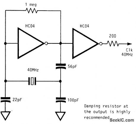
The circuit will operate reliably from below 1 MHz to above 400 MHz. With Vcc=5V the output of the second inverter essentially attains a full swing from O V to 5 V. Such large logic output levels and broad frequency range capabilities make this oscillator quite suitable for driving MOS components such as CPU, controller chip, peripheral devices, as well as other TTL products. A damping resistor in series between the clock output of the oscillator and the input of the device being driven will remove the undesirable undershoot and ringing caused by the high speed CMOS part. (View)
View full Circuit Diagram | Comments | Reading(2198)
HIGH_SPEED_DATA_ACQUISITION_SYSTEM
Published:2009/6/30 23:17:00 Author:May
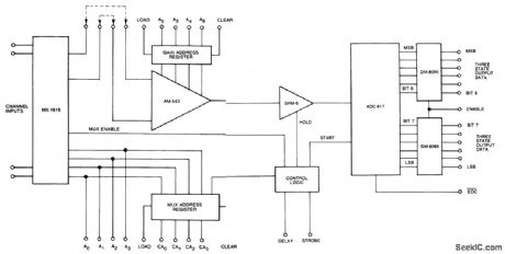
This diagram shows a high-speed data acquisition system with 8 differential inputs and 12-bit resolution using the AM-543. If the control logic is timed so that the Sample-Hold-ADC section is converting one analog value while the mux-amplifier section is al-lowed to settle to the next input value, throughout rates greater than 156 KHz can be achieved. The AM-543 is used with Datel's ADV-817, a 12-bit hybrid A/D with a 2 μSec conversion rate, the SHM-6, a 0.01%, 1 psec hybrid Sample-Hold, and the MX-1616,a low cost, high-speed monolithic analog multiplexer. The system works as follows:The μP selects a channel and initiates a conversion at G = 1 and then looks at the MSB of the conversion result. If the MSB = 1, the μP will store the value. If the MSB = 0, the μP will select G = 2. The μP will repeat the cycle of gain incrementing, comparison, and analog-to-digital conversion until the MSB = 1. The μP will then test for an output of all 1's, as this is the full-scale output of the A/D. If the output is all 1's, the μP will decrement the gain by 1 step and perform the final conversion.
(View)
View full Circuit Diagram | Comments | Reading(1562)
CMOS_DATA_ACQUISITION_SYSTEM
Published:2009/6/30 22:50:00 Author:May
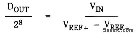
Charge redistribution to achieve A/D conversion. In typical applications, as a ratiometric conversion system for a microprocessor,VREF- will be connected to ground and VREF,+will be connected to VCC. The output will then be a simple proportional ratio between analog input voltage and VCC. The general relationship is:
Where DOUT=Digital Output VIN=Analog Input VREF=Positive Reference Potential VREF= Negative Reference Potential (View)
View full Circuit Diagram | Comments | Reading(824)
8048_IM8OC48_MICROCOMPUTER_WITH_8_CHARACTER16_SEGMENT_ASCII_TRIPLEX_LIQUID_CRYSTAL_DISPLAY
Published:2009/6/30 22:47:00 Author:May
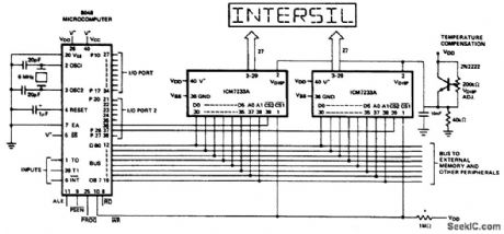
The two bit character address is merged with the data and written to the display driver under the control of the WR line. Port lines are used to either select the target driver, or deselect all of them for other bus operations. (View)
View full Circuit Diagram | Comments | Reading(1033)
Computer motherboard circuit diagram 440LX2_23
Published:2011/7/31 22:02:00 Author:Ecco | Keyword: Computer motherboard
View full Circuit Diagram | Comments | Reading(763)
Computer motherboard circuit diagram 440LX2_24
Published:2011/7/31 22:03:00 Author:Ecco | Keyword: Computer motherboard
View full Circuit Diagram | Comments | Reading(736)
Computer motherboard circuit diagram 440LX2_25
Published:2011/7/31 20:48:00 Author:Ecco | Keyword: Computer motherboard

View full Circuit Diagram | Comments | Reading(837)
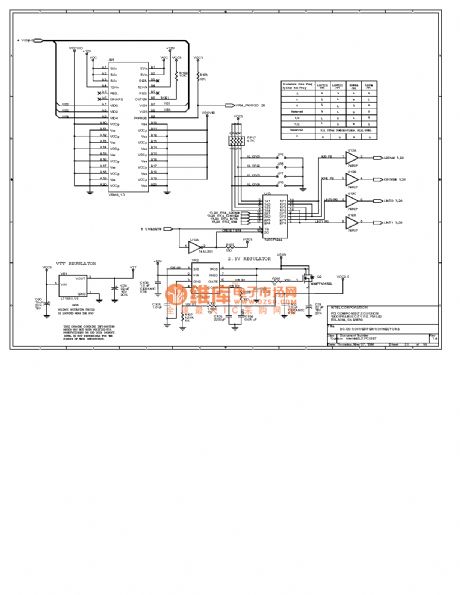
Computer motherboard circuit diagram 440LX2_26
Published:2011/7/31 20:39:00 Author:Ecco | Keyword: Computer motherboard
View full Circuit Diagram | Comments | Reading(852)
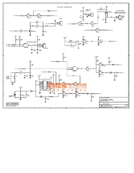
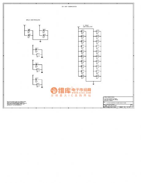
Computer motherboard circuit diagram 440LX2_28
Published:2011/7/31 20:48:00 Author:Ecco | Keyword: Computer motherboard
View full Circuit Diagram | Comments | Reading(775)
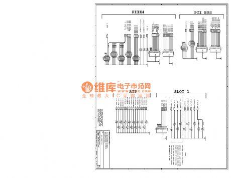
Computer motherboard circuit diagram 440LX2_29
Published:2011/7/31 20:40:00 Author:Ecco | Keyword: Computer motherboard
View full Circuit Diagram | Comments | Reading(767)
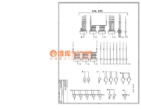
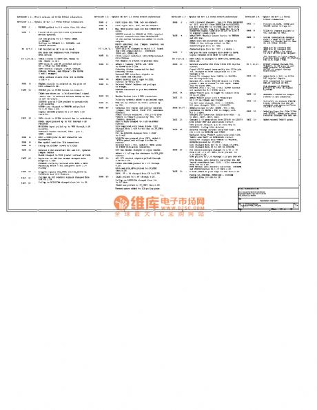
Computer motherboard circuit diagram 440LX2_30
Published:2011/7/31 20:41:00 Author:Ecco | Keyword: Computer motherboard
View full Circuit Diagram | Comments | Reading(736)
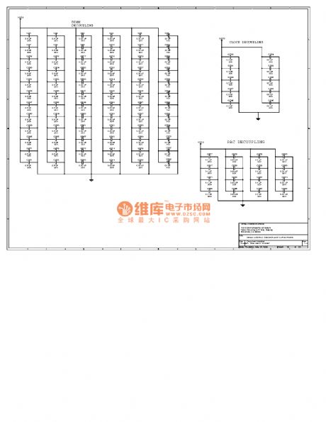
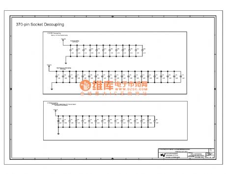
Computer motherboard circuit diagram 440LX2_31
Published:2011/7/31 20:42:00 Author:Ecco | Keyword: Computer motherboard
View full Circuit Diagram | Comments | Reading(737)
Computer motherboard circuit diagram 440LX2_32
Published:2011/7/31 20:42:00 Author:Ecco | Keyword: Computer motherboard
View full Circuit Diagram | Comments | Reading(777)
Computer motherboard circuit diagram 440LX2_33
Published:2011/7/31 20:43:00 Author:Ecco | Keyword: Computer motherboard
View full Circuit Diagram | Comments | Reading(750)
Computer motherboard circuit diagram 810 1_34
Published:2011/7/31 20:46:00 Author:Ecco | Keyword: Computer motherboard
View full Circuit Diagram | Comments | Reading(735)
| Pages:21/39 At 2021222324252627282930313233343536373839 |
Circuit Categories
power supply circuit
Amplifier Circuit
Basic Circuit
LED and Light Circuit
Sensor Circuit
Signal Processing
Electrical Equipment Circuit
Control Circuit
Remote Control Circuit
A/D-D/A Converter Circuit
Audio Circuit
Measuring and Test Circuit
Communication Circuit
Computer-Related Circuit
555 Circuit
Automotive Circuit
Repairing Circuit