
Battery Charger
Index 10
0.1C5A standard nickel-cadmium battery charger circuit of CD4541
Published:2011/6/20 6:09:00 Author:chopper | Keyword: 0.1C5A, standard nickel-cadmium battery, charger circuit
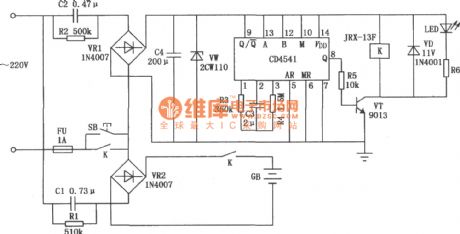
The following circuit makes use of the constant-current characteristic of capacitor and adopts pulsant direct current source to charge.Its effect is greater than pure DC,and it can charge one or more nickel-cadmium batteries.
(View)
View full Circuit Diagram | Comments | Reading(4746)
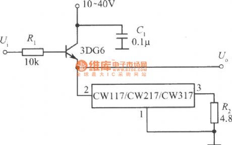
power follower of CW117/CW217/CW317 circuit
Published:2011/6/16 0:48:00 Author:chopper | Keyword: power follower
View full Circuit Diagram | Comments | Reading(1273)
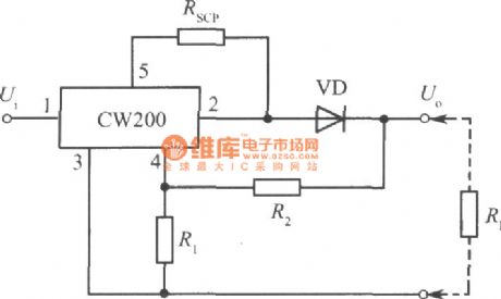
CW200 charger cirucit
Published:2011/6/16 22:07:00 Author:chopper | Keyword: charger
View full Circuit Diagram | Comments | Reading(788)
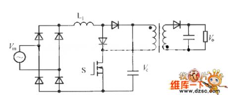
single-stage charging incentive-type PFC converter circuit
Published:2011/6/25 10:35:00 Author:John | Keyword: converter
View full Circuit Diagram | Comments | Reading(824)
Full-bridge single-stage PFC converter circuit
Published:2011/6/25 10:31:00 Author:John | Keyword: PFC converter
View full Circuit Diagram | Comments | Reading(879)
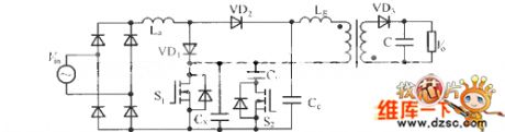
Boost Flyback-type single-stage isolated PFC converter circuit
Published:2011/6/25 9:40:00 Author:John | Keyword: converter
View full Circuit Diagram | Comments | Reading(1436)
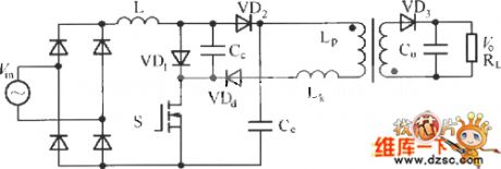
Basic Boost single-stage isolated PFC converter circuit
Published:2011/6/25 6:08:00 Author:John | Keyword: converter
View full Circuit Diagram | Comments | Reading(1303)
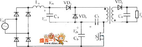
single-stage full-bridge PFC converter circuit
Published:2011/6/25 6:04:00 Author:John | Keyword: converter
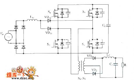
PFC technology has been gradually integrated into a lot of good converter circuits. The new developed structures can well suppress power supply to input harmonics, regulating the input current’s waveform. They also have excellent output characteristics, fully achieving the advantages of PFC circuit and power conversion circuit. The figure shows the single-stage PFC circuit formed by the Boost circuit and full-bridge converter. As for practical applications, the synthesis circuit improves the charging and discharging circuit of VDx1 and VDx2, thus leading to better functions.
(View)
View full Circuit Diagram | Comments | Reading(2577)
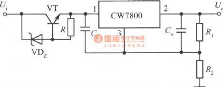
The high input-output integrated stable power supply circuit of CW7800 (2)
Published:2011/6/14 3:46:00 Author:Borg | Keyword: high input-output, power supply
View full Circuit Diagram | Comments | Reading(772)
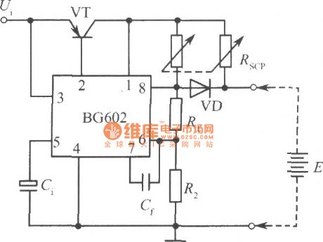
BG602 charger circuit
Published:2011/6/16 22:14:00 Author:chopper | Keyword: charger circuit
View full Circuit Diagram | Comments | Reading(844)
TL082 formed Ni-Cd battery automatic charge and discharge circuit diagram
Published:2011/6/1 5:12:00 Author:Crystal Liu | Keyword: Ni-Cd battery, automatic charge and discharge
This circuit can make two cadmium nickel battery 3V or discharge in charges to 1.34V. when charge or discharge circuit automatically cut off, effectively to preventthe phenomenon of charge or discharge. (View)
View full Circuit Diagram | Comments | Reading(2145)
LM324 formed after first discharge charge function battery charger diagram
Published:2011/6/1 5:10:00 Author:Crystal Liu | Keyword: after first discharge charge function , battery charger
This circuit in charge of cadmium nickel batteries before discharge,in order to eliminate memory effect,put the electric switch to automatically after charging status.Chargemode for width modulation constant flow,Pulse constant-current charge and pulse discharge,test battery ends voltage after filled,and a double control, parallel charge, with Counter-attack charge function.
(View)
View full Circuit Diagram | Comments | Reading(4564)
Ni-Cd battery charge circuit consist of CD4040
Published:2011/6/1 5:16:00 Author:Crystal Liu | Keyword: Ni-Cd battery charge circuit , CD4040
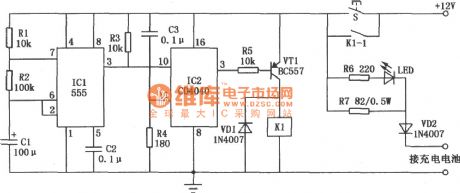
CD4040 counter chipformed the cadmium nickel battery charger as show in the picture. It can chargefor four quarter of cadmium nickel battery whoes capacity is 500mA , charge current charging time for 50mA, for l. five hours, and after finishing with charging the function of power. 555 time-based circuit constitute a clock signal generator, produce the l0Hz square wave signal, and its period for 6 seconds. When switching power supply, due to the 3 IC2 feet, so that the output low level VT1 semiconductor tube conduction, and make relay Kl suck close work, contact K1-1 closed, switch S in captive. Now charging current direction battery, and began to the battery. Status indicator LED lighted, said charging is ongoing.
CD4040 countermakes upfrequency divider and charging circuit. In the meanwhile, ICl switch on the power of the clock signal loss to produce the IC2 ⑩ feet, IC2 start counting. Because IC2 8192 was taken into the points: 1, therefore, only the frequency of an 8192 in counting pulse reach a IC2 feet by the (3) will only low level into high level, make VTl Kl stop work deadlines, and release the contacts K1-1, make it become disconnected from the state, bringing to a halt the charge. VD2 is used to prevent battery into circuit current reversed. (View)
View full Circuit Diagram | Comments | Reading(3253)
Produced by six-inverter DC / DC conversion circuit
Published:2011/5/27 7:07:00 Author:John | Keyword: six-inverter
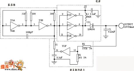
The circuit adjusts the voltage by controlling TTL switching threshold. U1A and U1B form the oscillator andtheoscillator'sswitching frequency is less than 1MHz. Output of oscillator drives three parallel inverters U1C, U1D and U1E. They can provide higher output current and output power. The internal output transistor, L1 and D1 form a standard boost converter. When the output is low, the current only flows through the inductor L1. When the output is higher, the energy stored in the inductor forces the anode of D1 to become higher. C1 conducts to charge D1.
(View)
View full Circuit Diagram | Comments | Reading(985)
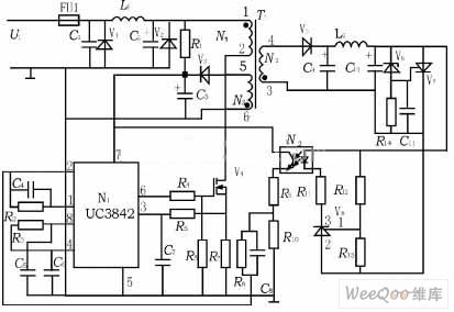
battery car charger production with low cost and high reliability circuit
Published:2011/5/27 7:08:00 Author:John | Keyword: battery car charger
Currently, MC3842 is the most widely used and the earliest single-ended drive for directly driving switch MOS FET. MC3842 can not put a stable voltage. At the same time, it also has a load current control. Thus, MC3842 is often referred as current control type switch power supply drive. There is no doubt that the charger has the unique advantage, resulting from features of MC3842. Only very few external components are needed to achieve constant pressure output. And the charge current can be controlled at the same time. Especially, that MC3842 can directly drive MOS FETsubstantially increase the reliability of the charger.
(View)
View full Circuit Diagram | Comments | Reading(1000)
Double closed loop control of electric bicycle charger circuit principle diagram
Published:2011/6/3 21:44:00 Author:Fiona | Keyword: Double closed loop control, electric bicycle charger
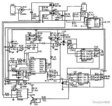
The charger is specifically designed for electric bicycle battery, it rectifys AC then uses IGBT to pressure regulating to achieve the charging voltage that the battery needs is about 3 6 V, control through the voltage and the current double closed loop to achieve the three-stage charging purposes. Chargers mainly consists of the major circuit and control circuit.The circuit principle is shown in the diagram. (View)
View full Circuit Diagram | Comments | Reading(3752)
Sawtooth Wave Generating Circuit with Optional Slope and Amplitude
Published:2011/6/6 1:06:00 Author:Michel | Keyword: Sawtooth Wave, Generating Circuit, Optional Slope and Amplitude
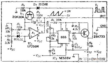
Circuit's FunctionsSawtooth wave can be used as scanning signals and it is a kind of waveform that voltage rises in linear way with the time. This waveform forms mostly by using capacitor constant-current charging and discharging method.This circuit changes output voltage and frequency through altering integration circuit's timing.Waveform slope can be setted by changing integration input current.
Circuit's Wrok PrincipleThe integrators A1 starts ponits in VR1 current when the power is switched on.The timer produces timing pulse according to certain time interval. (View)
View full Circuit Diagram | Comments | Reading(1150)
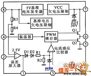
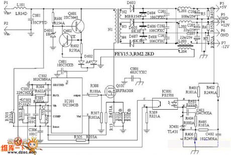
Typical Application Circuit of UC3842 Overvoltage and Overcurrent Protection
Published:2011/6/7 0:08:00 Author:Michel | Keyword: Overvoltage and Overcurrent Protection, Typical Application Circuit
The typical application circuit of UC3842 overvoltage and overcurrent protection picture is showed as above.
Overcurrent Protection Principle
When load current exceeds rating value or the output shorts,which causes that current is added to switch tube V4 ,R7's voltage feedbacks to feet.When R7's voltage exceeds 1V and the conduction width narrows down cuased by inside current amplifier and the output voltage drops,meanwhile it makes the UC3842 work's voltage drop.When it is lower thansetting voltage,over-current protection circuit starts to work to protect power tube.Power supply resumes work when short circuit phenomenon vanishes.
(View)
View full Circuit Diagram | Comments | Reading(10632)
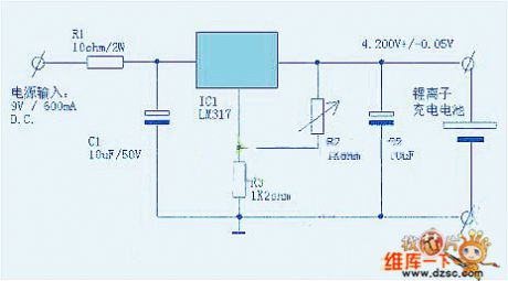
The simplest lithium battery charger circuit
Published:2011/6/3 20:03:00 Author:chopper | Keyword: lithium battery charger
View full Circuit Diagram | Comments | Reading(1433)
15W Triple Output DC / DC module power supply design circuit
Published:2011/5/24 0:05:00 Author:John | Keyword: DC / DC module power supply
DC / DC module has been widely used in railway communications, microwave communications, industrial control, marine electronics, avionics, ground radar, fire-fighting equipment and medical equipment, teaching equipment and many other fields. Many applications require multi-output, such as SCM intelligent controller. SCM needs power supply of 5V, while the op-amp usually needs power supply of 12V. During the design of multiple outputs, there are many different points from the single output. It is necessary to consider transformer pin constraints, multi-secondary transformer design and voltage regulator circuit achievement. It is also needed to consider the load rates for light load and full load of each channel and the characteristics for cross-load regulation.
(View)
View full Circuit Diagram | Comments | Reading(2501)
| Pages:10/13 12345678910111213 |
Circuit Categories
power supply circuit
Amplifier Circuit
Basic Circuit
LED and Light Circuit
Sensor Circuit
Signal Processing
Electrical Equipment Circuit
Control Circuit
Remote Control Circuit
A/D-D/A Converter Circuit
Audio Circuit
Measuring and Test Circuit
Communication Circuit
Computer-Related Circuit
555 Circuit
Automotive Circuit
Repairing Circuit