
Index 49
Single chip switching power supply design
Published:2011/11/13 21:59:00 Author:May | Keyword: Single chip, switching, power supply, design
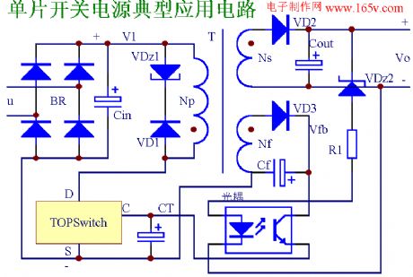
The typical application circuit of TOPSwitch series single chip switching power supply is shown in the diagram. High-frequency transformer in the circuit has three functions of energy storage, isolation output and voltage transformation. The diagram shows thatthe polarity of high frequency transformer primary winding Np is coincided with the opposite polarity of secondary winding Ns and the feedback winding NF. This indicates that the electrical energy is stored in the primary winding in the type of magnetic energy when TOPSwitch is broken over, and meanwhile VD2 is closed. When TOPSwitch is cut off, VD2 is broken over, energy will transfers to the secondary, namely, it is the features of fly-back switching power supply. In the diagram, BR is the rectifier bridge; Cin is the input end offilter capacitor. AC voltage u is rectified and filtered and then it will get DC high voltage V1. After passing the primary windings, it will add to the drain of TOPSwitch. In view of the TOPSwitch cut-off time, the spike voltage generated by drain of high frequency transformer can be superimposed on the DC high voltage V1 and the induced voltage Vor. It can make the brain voltage of power switching tube exceed 700V and damage the chip. So it must increase drain clamping protection circuit in the justified of primary winding. (View)
View full Circuit Diagram | Comments | Reading(3077)
Small switching power supply module using TOP222P
Published:2011/11/13 21:34:00 Author:May | Keyword: Small switching, power supply
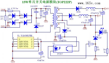

AC input voltage is 100~245V, double way DC output (note 1), the biggest output is separately 10V800mA, 5V800mA, and the power supply efficiency is 80%~89%. ( note 1: whenthe output is5V, this power supply module has the function of regulation voltage) (View)
View full Circuit Diagram | Comments | Reading(4826)
34063 used for DC-DC supply convert circuit
Published:2011/12/1 20:17:00 Author:May | Keyword: DC-DC supply convert
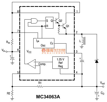
34063 is a kind of intergrated circuit which is used for DC-DC power supply converter.It canbeused for voltage boost, step-down and polarity reversed. The highest polarity reversed effect is 90%, the highest step-down effect is 80%, conversion efficiency and work frequency filter capacitorare indirect proportion. Moreover, when output power can not reach therequired value, for example, when >250~300MA, it can enlarge current through the method of external expansion power tube, andambipolar or MOS expansion current tube is ok.The peripheral cell nominal meaning and their value computing formula:Vout (output value)=1.25V(1+R1/R2)Ct (timing capacitor):decide internal operating frequency. Ct=0.000004*Ton (work frequency)Ipk=2*Iomx*T/offRsc (current-limiting resistance):decide output current. Rsc=0.33/IpkLmin(inductance): Lmin=(Vimin-Vces)*Ton/IpkCo ( filter capacitor): decide output voltage ripple factor, Co=Io*ton/Vp-p(ripple factor)fixed value parameter:Vces=1.0V ton/toff=(Vo+Vf-Vimin)/(Vimin-Vces) Vimin: minimum value when input voltage unsteadinessVf=1.2V high-speed switch diode forward voltage drop (View)
View full Circuit Diagram | Comments | Reading(2185)
MOSFET resonant DC-DC converter circuit diagram with high efficiency
Published:2011/7/27 22:44:00 Author:Nicole | Keyword: DC-DC converter, MOSFET
The figure is a MOSFET resonant DC-DC converter circuit. Luo Aiye circuit works through transformer magnetic saturation and make triode fliped. In this circuit, transformer works in nonsaturated mode, it changes with arc through the grid feedback voltage of MOSFET, and to make MOSFET fliped by reducing the grid voltage.
When it isconnected to input power supply,VT1 and VT2 are added grid bias by resistors R1 and R2, due to the inhomogeneity of grid voltage UTH (threshold voltage) when MOSFET is conduction, so the lower of UTH turns on firstly.
Assuming VTI turns on firstly, there are resonance current flowing between the capacitor C1 and primary coil 2 × Np, it is produced by LC, and C1 is connected to the both ends of transformer primary coil. This current adds resonance voltage to the drain-source of other MOSFET pipe VT2.
Since the resonant voltage drops in the grid feedback loop Nf, so it reaches 0V soon. When it is lower than the grid threshold of MOSFET VTl, VTl is off. However, the resonant voltage across OV and reverse negative, the grid of VT2 is positive biased and to be conducted. Of course, the grid voltage of VTl is negative, VTl keeps cut-off state at this time.
(View)
View full Circuit Diagram | Comments | Reading(6088)
Non-isolated switching power supply circuit diagram
Published:2011/7/27 22:44:00 Author:Nicole | Keyword: switching power supply
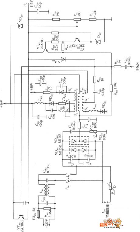
This is a useful non-isolated switching power supply circuit, it is used as the switching power supply of Peony TC - 483D color, including grid filter composed of C80l, C802, bridge rectifier circuit made of VD80l, VD802, a filter composed of R802, C807, peak voltage limiter composed of the varistor VD811; pulse oscillator consists of switch VT80l, pulse transformer T801; pulse width modulator made of VT802; error amplifier made of VT803.
It's not difficult to see from the figure, passing through the rectifier filter, 220V AC voltage is connected to output side directly by the primary winding of pulse transformer T801 and switch VT801, there is no isolation. The power supply has 16V, 50V and 113V three kinds of DC voltage output. When VT80l turns on, 113V DC output voltage will supply power to the load, while store electrical energy in C814 and magnetic energy in T801. When VT80l cut off, the N1 ~ N3 windings will produce the induced voltage with left negative and right, to make VD805 positive-skewed on, the energy stored in transformer will supply power to the load and charge to C814; C814 and L80l composition filter circuit, to make the 113V output voltage continuous and smooth.
(View)
View full Circuit Diagram | Comments | Reading(2354)
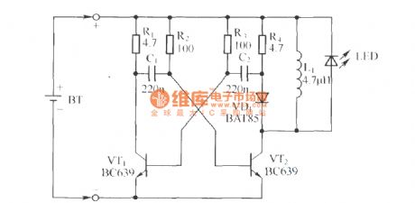
Light-control electric toy circuit
Published:2011/7/28 1:31:00 Author:Nicole | Keyword: electric toy
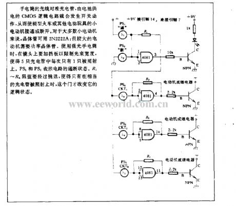
The light of flashlight aims at phototube, then CMOS logic circuit which adopts battery as power supply will occur switch action to turn on/off the motor of model train or other electric toys. To most small motor, the transistor can use 2N2222A; but the larger motors need power transistor. When using highlightflashlight, to add a baffle to lens to limit the width of light beam, then only one of phototubes will be shone. PS1 and PS2 represent the on/off state of circuit. R1~R4 resistance should be selected, only the matching phototube is shone, this gate will change its logic state. (View)
View full Circuit Diagram | Comments | Reading(1933)
Photoelectric isolating quick switch circuit
Published:2011/7/28 1:27:00 Author:Nicole | Keyword: Photoelectric, isolating quick switch
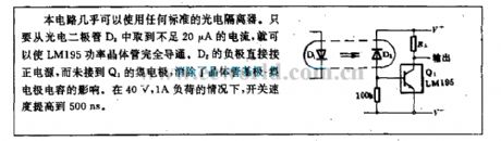
Nearly any standard photoelectric isolator can be used in this circuit, it just needs about 20μA current from photodiode D2, then the LM195 power transistor can be turned on. The negative of D2 connects to positive power supply directly, it is not connected to Q1's collector, then the influence of transistor base-collector on capacitance will be eliminated. In the case of 40V, 1A load, the speed of switch can be improved to 500ns. (View)
View full Circuit Diagram | Comments | Reading(926)
Light pen interface circuit
Published:2011/8/10 3:57:00 Author:Nicole | Keyword: light pen, interface circuit
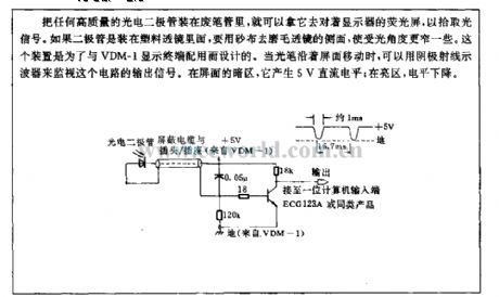
Whatever high quality photoelectric diode is fixed into exhaust pen pipe, it can face to the display screen to pick up light singal. If the diode is put in plastic lens, then it should use carbasus to sand the side of lens andto narrow the received light angle. This device is designed for matching VDM-1 display terminal. When light pen moves along the face of the screen, it can use a cathode ray oscillograph to monitor the output singal. In the dark space of screen, it will produce 5V DC level; in bright area, the level drops. (View)
View full Circuit Diagram | Comments | Reading(1158)
Ni-Cd battery discharger circuit
Published:2011/8/10 3:57:00 Author:Nicole | Keyword: Ni-Cd battery, discharger
The greatest shortcoming of Ni-Cd battery is: it has memory effect, an effective method to eliminate memory effect is: to fully discharge the Ni-Cd battery before its third or fourth charge, that is charging to Ni-Cd battery after its single section voltage drops to 0.75V, this way can make Ni-Cd battery recover capacity in time then to ensure it for normal use, but the final voltage of every single section Ni-Cd battery shouldnot belower than 0.65V, or else Ni-Cd battery will be polarity reversed and damaged due to over discharge.
(View)
View full Circuit Diagram | Comments | Reading(1742)
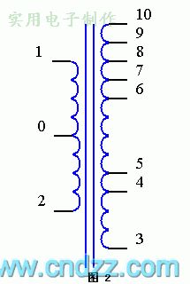
1kW switching power supply transformer
Published:2011/12/5 1:05:00 Author:May | Keyword: 1kW, switching power supply, transformer
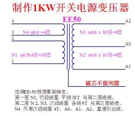
It selects the EE-50 determined according to the skeleton .The first layer N1, the primary coil is wound flatly with 38T, and it is insulated with the second layer. The second layer N2, N3, secondary are wound with 9T, and it is insulated with the third level. N4 fan secondary is wound with 4T. A0, A1, A2 are direct pinouts.
(View)
View full Circuit Diagram | Comments | Reading(1491)
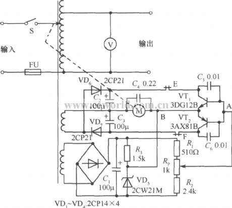
200W automatic voltage adjustment type AC stabilized voltage supply circuit diagram
Published:2011/12/1 20:32:00 Author:May | Keyword: 200W, automatic voltage adjustment, AC, stabilized voltage supply
View full Circuit Diagram | Comments | Reading(1716)
20V regulated power supply circuit
Published:2011/12/2 0:19:00 Author:May | Keyword: 20V, regulated power supply
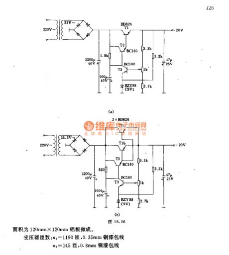
The maximum wasted power of compensating pipe T1 shown in diagram (a) is 5.6W. The radiator of compensating pipe T1 can be made by aluminium plate with 2mm thick and 100mm×100mm area. Need regulated voltage can be adjusted to 20V by 1kΩ regulation resistor which is connected at base of transistor T3.
transformer winding number: n1=1600turns, 0.25mm copper lacquered wire n2=180turns, 0.7mm copper lacquered wire
The maximum wasted power of compensating pipe T1a and T2b shown in diagram (b) can reach 14.5W. Each transistor radiator can be made by aluminium plate with 2mm thich and 120mm×120mm area.
transformer winding number: n1=1190turns, 0.35mm copper lacquered wire n2=145turns, 0.8mm copper lacquered wire
(View)
View full Circuit Diagram | Comments | Reading(1660)
100W VMOS pipe inverted power supply circuit
Published:2011/12/1 20:45:00 Author:May | Keyword: 100W, VMOS pipe, inverted power supply
The circuit of this system is simple and easy to debugging. The performance of this system is reliable. This system can automatically converting, inverting and charging. It also has jar battery indicator. Thanksfor adopting high power VMOS pipe, its efficiency is high and its cost is lower. This system is fit for electrophile assembling and installing.
The circuit working principle is shown in diagram 1. Multivibrator consists of VT1 and VT2. Its oscillator frequency is 5Hz. When voltage decreases, in order to get the same frequency, the power supply of oscillator is regulated by voltage regulator tube VD1. The square-wave voltage isoutput by multivibrator, then it directly pushes VMOS high power pipe. The 220V AC isset up by transformer and extract from socket CZ.
(View)
View full Circuit Diagram | Comments | Reading(1252)
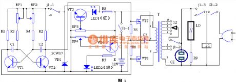
The production circuit diagram of Performance reliable high power switching power supply
Published:2011/11/21 21:49:00 Author:May | Keyword: Performance reliable, high power, switching power supply
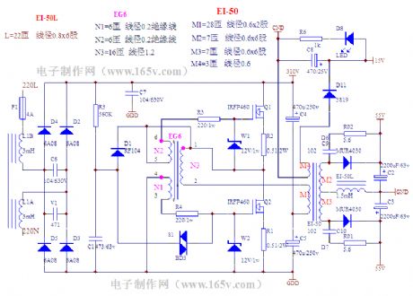
This circuit is a simple and reliable high power switching power supply. Theproduct is designed by a factory. It is applied in large light. Some explanation of this transformer is in the following:
(EI-50L) is storage power inductor. It adopts EE-50 magnetic core or EI-50 magnetic core. EI-50 magnetic core is output transformer. You can produce according to the explanation in the circuit diagram. EG6 is magnetic ring with 12mm diameter. The coiling is also made according to the explanation in the circuit diagram.
No-load running test is less than 20mA. The transfer efficiency is more than 90%. The maximum power is 800W. ( when 60V/13.5A, the input AC is 3.1A) (View)
View full Circuit Diagram | Comments | Reading(4002)
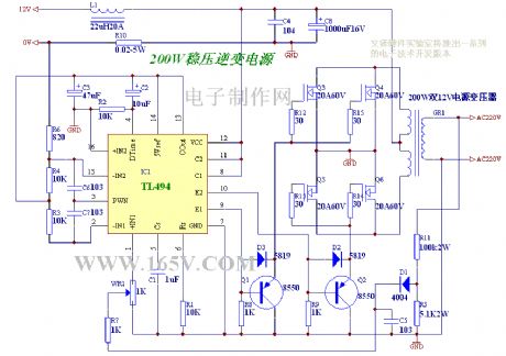
TL494 control car audio inverter power supply
Published:2011/11/10 2:16:00 Author:May | Keyword: control, car audio inverter, power supply
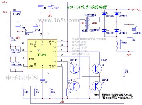
TL494 controls car's audio inverter power supply: it is high-fidelity audio power supply of custom car.It can work reliably without adjusting according this circuit diagram set. (View)
View full Circuit Diagram | Comments | Reading(16707)
Stabilized voltage inverter 12V-220V 200W
Published:2011/11/22 1:37:00 Author:May | Keyword: Stabilized, voltage inverter, 12V-220V 200W
Stabilized voltage inverter 12V-220V 200W is shown in the following diagram. It can adopt existing dual 12V-200W mains transformer. But its invert efficiency is low.
(View)
View full Circuit Diagram | Comments | Reading(8691)
The simplest practical switching power supply (one triode)
Published:2011/11/22 1:37:00 Author:May | Keyword: simplest practical, switching power supply, one triode
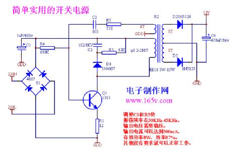
It can make the frequency bein the range of 30kHz-45kHzby adjusting C3 and R5. Output voltage needs to be regulated voltage. Output current can reach 500mA. Effective power is 8W. Efficiency is 87%. This circuit can worknormally with non requirement about others. (View)
View full Circuit Diagram | Comments | Reading(2387)
The power supply circuit diagram of ENVISION EC-1468 SVGA multiple frequency color display
Published:2011/11/10 2:07:00 Author:May | Keyword: power supply, ENVISION, SVGA, multiple frequency, color display
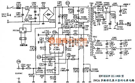
View full Circuit Diagram | Comments | Reading(1567)
The power supply circuit diagram of FUJITSU FMV-DPS84Y2 SGVA color dispaly
Published:2011/11/10 2:08:00 Author:May | Keyword: power supply, FUJITSU, color dispaly , SGVA
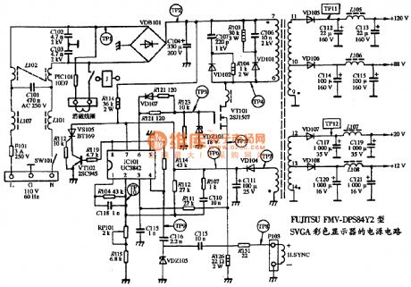
View full Circuit Diagram | Comments | Reading(2093)
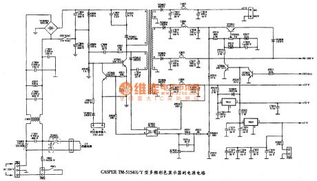
The power supply circuit diagram of CASPER TM-5154H SVGA multiple frequency color display
Published:2011/11/10 2:10:00 Author:May | Keyword: power supply, CASPER, SVGA, multiple frequency, color display
View full Circuit Diagram | Comments | Reading(1450)
| Pages:49/291 At 204142434445464748495051525354555657585960Under 20 |
Circuit Categories
power supply circuit
Amplifier Circuit
Basic Circuit
LED and Light Circuit
Sensor Circuit
Signal Processing
Electrical Equipment Circuit
Control Circuit
Remote Control Circuit
A/D-D/A Converter Circuit
Audio Circuit
Measuring and Test Circuit
Communication Circuit
Computer-Related Circuit
555 Circuit
Automotive Circuit
Repairing Circuit