
Index 51
Frequency modulation type switching stabilized voltage supply 1
Published:2011/11/22 0:27:00 Author:May | Keyword: Frequency modulation, switching, stabilized voltage supply
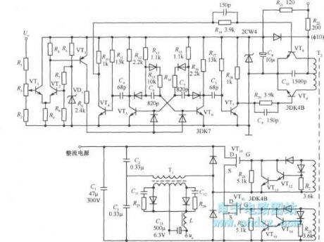
In the diagram, VT5 and VT6 make up the impulse oscillator. It has high response speed and wide frequency adjustable range. The reason is that the base driver and timing loopare separating, and they can work by themselves without disturbing. Frequency regulation is finished by comparator amplifier composed of VT1, VT2 and VT3.
Power switching tubesare VTT10, VT11 VMOS tubes. It can make influence onthe switching tube turning on speed and cutting off speedif input capacitor is too high. In order to overcome this problem, we can add a compensation circuit composed of R22 and CI0 on the primary of isolation transformer T2. After that, when the circuit is open, the primary of T2 has a higher voltage about 18V; when the tube is closed, the amplitude is already dropped down. It has about 11V voltage. When the circuit is open in the next time, the amplitude is already recovery again. (View)
View full Circuit Diagram | Comments | Reading(1003)
Hitachi NP8C power supply
Published:2011/11/22 0:19:00 Author:May | Keyword: Hitachi, power supply
The models using Hitachi NP8C power supply are: Hitachi CTP236, CEP320D, CRP350D, 450D, Furistock HFC-236, 450, Goldstar C37-401, C46-1, C563, etc. This power supply is widely used for early period color TV in China.
Oscillating process
300V DC voltage is added to switching tube Q901's B pole through R911, R907 and R908. Q901 starts to break over. T901's primary winding has current, at the same time, it can generate induction voltage, its polarity is that up is positive and down is negative. So this stage winding also can generate induction voltage, the polarity is thatdown is positive and up is negative. This voltage is sending to Q901's B pole through R902, R909 and C908, and it can make Q9021 break over further, the strong positive feedback makes Q901 rapidly saturation. (View)
View full Circuit Diagram | Comments | Reading(3341)
Practical circuit of full bridge switching stabilized voltage supply
Published:2011/11/14 2:37:00 Author:May | Keyword: full bridge, switching, stabilized voltage supply
The diagram is practical circuit of full bridge switching stabilized voltage supply. It is 1500W double pole power switching stabilized voltage supply circuit controlled by CW194. In the circuit, four double pole high back voltage transistors F661 are switching tube. Controlled by integrated circuit CW494, two pairs tubes are breaking over and cutting off in turns. It can change DC to high frequency AC. Then the high frequency AC is passing high frequency transformer to step-down. After rectifying and filtering, it will get 12V DC stabilized voltage. F661 power switching tube's BVceo≥400V. Time of toff is 1μs. So in the conditionwith high power, its power consumption is small.
The core component of this circuit is high-frequency transformer. Its magnetism performance has high requirement: frequency characteristic requires to reach megahertz; saturation magnetic flux density must reach to 5000Gs; magnetic hysteresis loss must be small; when it uses EC70 magnetic core, output power is 1000W; when it uses EC90 magnetic core, output power is 2000W. (View)
View full Circuit Diagram | Comments | Reading(1660)
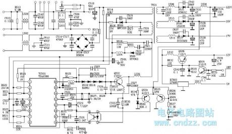
Jinxin TDA two chip system power supply
Published:2011/11/14 3:31:00 Author:May | Keyword: Jinxin TDA, two chip system, power supply
This power supply is also known as X53P power supply or X56P power supply. Taking Jinxing C498 for example, we simply introduced the principle of working.
Oscillating process
About 300V DC voltage on C708 adds to B pole of switching tube V720 by R729, R731 and L711. V720 starts to turn on. C pole's current is enlarging. T705's pin 1 and 12 generate induced electromotive force. Its polarity is that 1 is positive and 12 is negative. The positive feedback winding also generates negative induced voltage. Its polarity is 10 is positive and 9 is negative. This feedback voltage is added to B pole of V720 by C713, V713 and R713. It can make V720's current increase. Looping like this can make V720 saturation rapidly.
Voltage regulation process
Voltage regulation circuit consists of V745 and peripheral components. The sampling winding is T705's 7 and 8 winding. The voltage passes through V741 rectifying and C745 filtering. The voltage on C745 reflects the size of output voltage. If output voltage is increasing, the voltage on C745 is increasing too. (View)
View full Circuit Diagram | Comments | Reading(1033)
Switching power supply type high voltage constant current source circuit diagram
Published:2011/11/14 1:58:00 Author:May | Keyword: Switching power supply, high voltage, constant current source
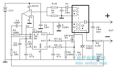
To develop a device instrument, we need a constant current source which can generate 1MA current on the resistor with the resistance value of0~3MΩ. We designed one by using UC3845 and 12V storage battery. Transformer adopts color TV high voltage package. L1 uses enameled wire to go around 24 turns on original high voltage package magnetic core. L3 gets help from one turn of original high voltage package. L2 gets help from high-voltage parts of high voltage package. Voltage limiting circuit consists of L3 and LM393. It can limit the output voltage and make it not too high. It can adjust the voltage of open circuit by adjusting R10. (View)
View full Circuit Diagram | Comments | Reading(7259)
Kaige 4C7108 power supply
Published:2011/11/14 2:03:00 Author:May | Keyword: Kaige, power supply
Kaige 4C7108 adopts separated exciting single-end fly-back converter type switching power supply. Oscillating circuit adopts TDA83820. Main power supply output voltage is 115V.
Voltage regulator circuit
Voltage regulator circuit mainly consists of components of Q503, Q504, IC502, etc. Difference amplifier composed of Q503 and Q504, whichare error sampling circuit. D519 offers reference voltage for Q503. B pole of Q504 changes along with output voltage. When output voltage is too high, the break over level of Q504 is decrease, and Q503's C pole current is dividing, then it will decreasing. The current of IC502 is increasing. Internal resistance of IC502's pin 4, 5 is decreasing. The voltage of IC501's pin 9 is decreasing. The duty factor of widened pulse is decreasing. Then output voltage is decreasing. So it reaches the purpose of voltage regulation. It can change output voltage by adjusting VR504. (View)
View full Circuit Diagram | Comments | Reading(1842)
Controlled silicon switching stabilized voltage supply
Published:2011/11/14 2:30:00 Author:May | Keyword: Controlled silicon, switching stabilized voltage supply
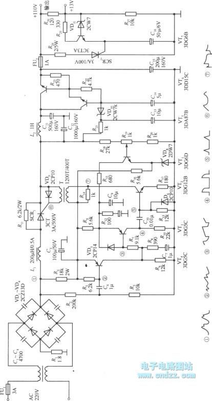
When controlled silicon switching stabilized voltage supply is normal working, it uses very small control currentto control very high anode current.
The diagram showsa practical circuit of controlled silicon ripples trigger type switching stabilized voltage supply. It shapes and enlarges of rectified ripple. Then it can trigger controlled silicon and make it break over. When the momentary value of rectified voltage is dropping to 0V, controlled silicon will becut off byitself. It can achieve voltage regulation by using the changes of output voltage to control the leading edge of trigger pulse.
Voltage regulator circuit mainly consists of transistors VT1~VT4, transformer T, controlled silicon SCR1, etc.
When the power supply turns on, rectifier can output pulse DC voltage like wave ①. It adds to the base of VT4 after diving by R2 and R3, the wave is shown in ②. VT4 can enlarge it, then collector output pulse can charge to C7 through R8, so it can generate run up saw-tooth wave. The wave is sent to the base of VT3 through R7, its wave is shown in ③. (View)
View full Circuit Diagram | Comments | Reading(1033)
Switching voltage regulator of Jinxin brand TV
Published:2011/11/14 3:33:00 Author:May | Keyword: Switching voltage regulator, Jinxin brand TV
Switching power supply with input and output isolation normally has three forms: transformer isolation, photoelectric coupling isolation and sampling and output segregating isolation.
Switching voltage regulator of Jinxing brand is shown in the diagram. It adopts two transformers. Sampling circuit R1, Rp and R2 directly connect to the output end of power supply. It can sample from 120V output voltage to a scale and add to the base of error amplifier VT1. This voltage and the reference voltage offered by VD1 and R5 are compared and enlarged by VT1. Then the collector is outputting error voltage. It is direct coupled by R7 and giving it to pulse width modulation circuit composed of Schmidt trigger VT2 and VT3. Then it is changed to pulse. The pulse is enlarged by VT4. It can realize total isolation except switching output stage. Its sound insulation is perfect. What’s more, we should use a transformer T1.
(View)
View full Circuit Diagram | Comments | Reading(1307)
Jinxin C7428 power supply
Published:2011/11/21 20:40:00 Author:May | Keyword: Jinxin, power supply
C7428 power supply adopts wide voltage design. It can adapt 110V-245V network voltage. It is similar to Toshiba 2500XH power supply.
Network input switching circuit
In order to adapt11V-245V network voltage, this power supply is designedfor freely switch over voltage multiplying rectifier and bridge rectifier. The power supply adopts multiplying rectifier when network input voltage is lower than 145V. It adopts bridge rectifier when network input voltage is higher than 145V.
Network input voltage is firstly rectified by V801, V802to get identification voltage on C808 after low-pass filtering. The identification voltage is added to STR81145's pin 2, 5. If network input voltage is lower than 145V, thevoltage on thetwo ends of C808 is lower. STR81145's pin 2, 3are breaked over. At this time, V803 and C818, C819 make up multiplying rectifier. The circuit has over voltage protection circuit in order to prevent STR81145's error identification. (View)
View full Circuit Diagram | Comments | Reading(1949)
Simple ringing choke type switching stabilized voltage supply
Published:2011/11/21 21:19:00 Author:May | Keyword: ringing choke type, switching, stabilized voltage supply
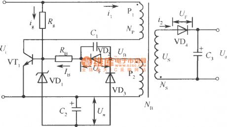
Ringing choke type is a kind of self-oscillation feedback converting model. Its basic principle is shown in the diagram. When it adds input power supply, the current passes Rg and flows to the base of switching tube VT1 to make VT1 break over. At this time, thediode of transformer secondary polarity is in reverse bias. The diode has no current. So the current of VT1 collector and transformer winding Np is the same. Rg is called starting resistor.
Once VT1 is breaking over, transformer primary winding Np is added input voltage, and coil NB also generates induction voltage UB. Also, coil NB adds current IB to the base of VT1to make VT1 further breaking over.
Transformer generates electromotive force, of which the polarity is the contrary of input voltage's polarity. When VT1 is cutting off, its power is the samewith thetransformer before VT1 is cut off.
The diode of transformer secondary polarity is breaking over due to the function of reverse electromotive force. The power transformer stored in unit time is equal to output power. (View)
View full Circuit Diagram | Comments | Reading(3433)
Reduced voltage type chopping type switching stabilized voltage supply principle diagram
Published:2011/11/14 0:26:00 Author:May | Keyword: Reduced voltage type, chopping type, switching stabilized voltage supply
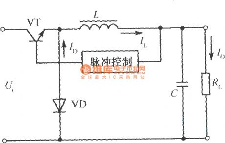
Chopping switching stabilized voltage supply is DC energy supply. It can get single-direction square wave after passing switching circuit. Then it can get stable DC which is different with input voltage after filtering. Soit means that whether input voltage Ui is positive or negative, output voltage Uo is always lower than input voltage Ui, that is | Uo|≤|Ui|. The diagram shows reduced voltage chopping type switching stabilized voltage supply principle diagram. When switching component VT is controlled and saturation conduction, the energy is stored in inductor L and capacitor C. When switching component T is controlled and in the cut-off state, the energy stored in inductor and capacitor is still offered to load, and the diode CD makes up the current loop. It is also called series switching stabilized voltage supply because switching component VT and load resistor RLare connected inseries. (View)
View full Circuit Diagram | Comments | Reading(928)
High voltage switching stabilized voltage supply circuit
Published:2011/11/13 21:48:00 Author:May | Keyword: High voltage, switching, stabilized voltage supply
High voltage switching stabilized voltage supply circuit is shown in the diagram. It is the switching power supply of 80P type color TV. It adopts auto-excitation, PWM circuit. Its output is isolated with power system. This power supply has 110V and 18V DC voltage output. The power supply consists of power frequency rectification filtration circuit, start oscillating circuit, control circuit and DC output circuit.
Input filter composed of capacitors C309, C301 and inductor L301 to weaken the power system interference of power supply. It also can prevent power supply from interfering and polluting. Power frequency rectification filtration circuit composed of VD301~VD304 tochange 220V AC voltage into about 300V DC current. The usage of C304~C307 is to protect the diode form being parallel with them. 300V DC voltage passes starting resistor R302 to reduce voltage, then it will be added to the base of switching compensating pipe VT304, which canmake it to get positive bias and turn on. At the same time, the end of input winding ⑨~② pulse transformer T301 has current. It makes feedback winding 11~⑩ end get positive feedback. (View)
View full Circuit Diagram | Comments | Reading(3263)
Single-ended Foward Transforming Switching Regulated Power Supply Application Circuit
Published:2011/11/13 21:55:00 Author:May | Keyword: Single end, positive energize, converter type, switching, regulated power supply
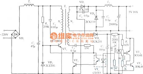
The diagram is single-ended Foward Transforming Switching Regulated Power Supply Application Circuit. The isolation effect is good because it adopts photo-coupler in the feedback loop. The output voltage of this power supply is 5V. The output current is 10A. When the power supply is broken over, it will output 300V DC voltage through the rectifying and filtering of VD1, L1, C1. It is added on switching tube VT1 directly, and it will provide a working voltagefor control circuit tomake it work.
During the switching tube VT1 is breaking over, the secondary winding N2 of transformer T gets energy. Its polarity can make rectifier diode VD3 breakover.
When output voltage Uo is increasing due to some reasons, the current of VT4, VT5 is increasing. This current is coupling to VT2 through photo-coupler VT3, it can decrease the internal resistance of VT2, thereby the base potential of control switching tube VT1 is decreasing, VT1's duty factor is decreasing, Uo is dropping down.
(View)
View full Circuit Diagram | Comments | Reading(1059)
Practical power supply of single end fly back type switching regulated power supply
Published:2011/11/14 3:29:00 Author:May | Keyword: single end, fly back type, switching, regulated power supply

The following diagram is a practical power supply of single end fly back type switching regulated power supply. It adopts CW3840 pulse width modulation integrated circuit to control. At present, CW3840 is pulse width modulation with many functions. Its internal circuit including precise power supply, oscillator, error amplifier, over voltage and over current comparator, slop generator, pulse width modulation and slow starts and program control circuit, etc.
AC main supply voltage 220V (or 110V) passes bridge rectifier VD1 to rectify and C1, C2 to filter. Then it will generate 300V DC voltage. The voltage pass resistor R3, R4 to reduce voltage. Then it will add to CW3840's 15 end and as working voltage. CW3840's working voltage slowly increased to 12V because of capacitor C3. This voltage passes R7, R8 to divide voltage and add it to 2 end of over voltage comparator. The threshold value of this comparator is 3V. When 2 end voltage is less than 3V, comparator outputs low level. It can make the drive transistor on integrated circuit cutting off and starts latch is locking. It indicated under voltage error. It also makes 8 end and capacitor C9 to be low level. Protective power supply is slow starting.
(View)
View full Circuit Diagram | Comments | Reading(1188)
TOP209/210 pin configuration
Published:2011/11/14 3:22:00 Author:May | Keyword: pin configuration
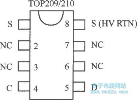
TOP209/210 series is a kind of highly efficient, low-power, pulse width modulated type three-terminal chip switching power supply successfully developed by Power Company in 1997 and is suitable for Stand-by Power of small power switching power supply with less than 8W power or electrical equipment.
TOP209/210 has two kinds of package: 8 foot dual inline (DIP-8) and 8-pin surface mount (SMD-8). Pin configuration is shown in the diagram. It is still equivalent to three-terminal devices because pin 2,3,6,7 all are empty (NC). Pin 1 and pin 8are connected inside. The only difference is pin 1 is connected with external bias / feedback Back to bypass capacitor terminal and control the negative side and pin 8 is external connected with high back end of the primary grade (HVRTN) when designing PCB. Pin 4 is connected with control end and pin 5 is connected with drain end. Its working principle is the samewith TOP100. But we must explain that: (1) TOP209's switching frequency is changed to 70kHz, and the switching frequency of TOP210 is still 100kHz; (2) both ofthe thermal shutdown temperatureis 145°C, and it is 10°C higher than TOPSwitch - Ⅱ's; (3) TOP209/210's limiting current values separatelyare 0.15 ~ O.23A, 0.23 ~ 0.30A; (4) Power MOSFET's withstand voltage is 700V.
(View)
View full Circuit Diagram | Comments | Reading(1565)
ZVT soft-switching PFC switching regulated power supply circuit
Published:2011/11/14 2:42:00 Author:May | Keyword: ZVT soft-switching, PFC, switching regulated power supply
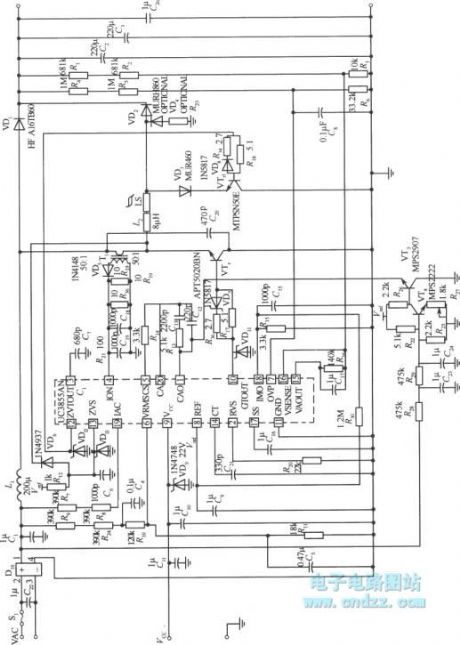
The diagram is power factor adjustment (PFC) switching regulated power supply circuit using zero-voltage converter (ZVT) soft-switch technique. Compared with hard switching active power factor adjustment (PFC) circuit, this circuit has one more out of auxiliary switch tube and resonant circuit. Main switching tube VTr and auxiliary switch VTr1 can becontrolled by a piece of IC chip-UC3855AN.
In the diagram, auxiliary switch and resonance LC circuit can make main switch tube achieve ZVT soft switch working. UC3855AN outputs two ways pulse trains, and they separately control the turning on of main switch tube and auxiliary switching tube. The computation of its feedback sampling and duty factor is the similar to UC3854.
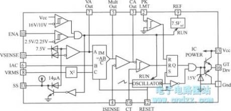
The internal structure of UC3854 single chip integrated circuit is shown in the following diagram. It mainly consists of voltage amplifier, analog multiplier, current amplifier and the composition of fixed-frequency pulse width modulator. in addition, it contains gate driver which is compatible with power MOSFET, 7.5V voltage reference, load enabling comparators, voltage detection and over-current comparator. UC3854 can accurately keep the sine ratio of bus input current with no need to slop compensation to the current.
(View)
View full Circuit Diagram | Comments | Reading(1881)
Switching regulated power supply using 110V (doubling voltage)/220V AC voltage input
Published:2011/11/13 21:33:00 Author:May | Keyword: Switching regulated power supply, 110V (doubling voltage)/220V AC voltage input
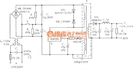
This power supply circuit is shown in the diagram. Its input AC voltage is 110V or 220V. When 110V AC voltage power supply changesin the range of 85~132V or 220V AC voltage power supply changes at the range of 170~265V, Sv=±1%. When the changing range of load current is 10%~100%, Si=5%, output ripple voltage is ±50mV. S in the circuit is 110V/220V AC voltage option switch. It can use cable jumper on printed plate to replace switch. When S is closed, it chooses 110V AC voltage as input, at this time, voltage doubling rectifying circuit consists of rectifying bridge BR and resistor capacitor components R1, C1, R2 and C2. When S is cut, it chooses 220V AC voltage as input. It added resistor R4 in output circuit in order to improve the voltage stability when it is atlight load. The smallest load current set by it is 36mA.
(View)
View full Circuit Diagram | Comments | Reading(3688)
Switching power supply of Beijing brand black and white TV
Published:2011/11/13 21:28:00 Author:May | Keyword: Switching power supply, Beijing brand, black and white TV
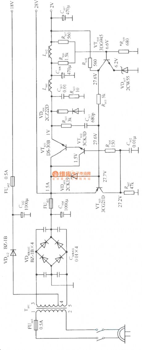
The diagram shows switching regulated power supply of Beijing brand white and black TV. It is a typical example of low voltage switching regulated power supply.
This power supply has three ways of DC output that is 18V, 28V and 12V. Among them, 28V is directly outputted by bridge type rectifier; 12V is output after 28V voltage beingregulated by switching voltage regulator; 18V is output by half wave rectifying and filter circuit.
VZ601 is switch power adjustable tube. Self-excited harmonic oscillator consists of VT601~VT603, R601, C601, etc. This power supply belongs to pulse width modulation type switching regulated power supply. When 12V voltage isincreased because of some reasons, the base potential of error amplifier tube VT601 is increased. Its collector potential is decreased, base potential of VT603 is also decreased, the output pulse width of switching adjustable tube VT601 is narrow, it makes increased voltage decreased again. (View)
View full Circuit Diagram | Comments | Reading(1484)
Simplified principle diagram of non-isolation switching power supply
Published:2011/11/13 21:21:00 Author:May | Keyword: non-isolation switching, power supply
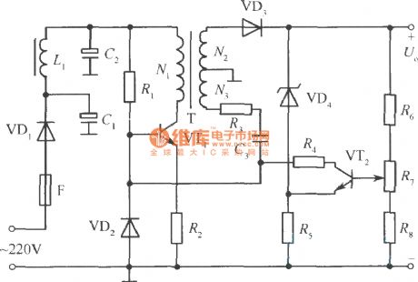
In high-voltage switching power supply, it cancels power frequency transformer with isolation effect, and it isshown in the diagram. It is simplified principle diagram of switching power supply which is non-isolation with network. Switching tube VT1 is connectedto network through rectifier, the switching tubehas electrification. Switching tube can couple the energy to output end through high-frequency transformer. Because output end and input end have the same earth point andare directly connected with error amplifier VT2 connected in output end and switching tube VT1, output end is breaking over with network through output end. (View)
View full Circuit Diagram | Comments | Reading(1394)
Homemade multi-functional thyristor charger circuit
Published:2011/11/13 21:02:00 Author:May | Keyword: Homemade, multi-functional, thyristor, charger circuit
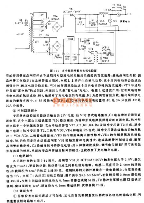
Working principleThis set mainly consists of major loop and conttrol loop. The circuit is shown in diagram 5-14.(1)major loop part (charge loop part)Commercial power 220V passes transformer T1 and reduction voltage. Secondary major loop winding have five taps. Among them, S2-1 charges to 6V storage battery, S2-2 charges to 12V storage battery or charges to 6V storage with heavy current, S2-3 charges to 18V storage battery or chareges to 12V storage battery with heavy current, S2-4 charges to 24V storage battery.This voltage is controlled and output by thyristor. The output end connectsto fly-wheel diode VD5 and filter inductance L.(2) control loop partTransformer's secondary control loop winding can output 23V voltage. (View)
View full Circuit Diagram | Comments | Reading(1622)
| Pages:51/291 At 204142434445464748495051525354555657585960Under 20 |
Circuit Categories
power supply circuit
Amplifier Circuit
Basic Circuit
LED and Light Circuit
Sensor Circuit
Signal Processing
Electrical Equipment Circuit
Control Circuit
Remote Control Circuit
A/D-D/A Converter Circuit
Audio Circuit
Measuring and Test Circuit
Communication Circuit
Computer-Related Circuit
555 Circuit
Automotive Circuit
Repairing Circuit