
Amplifier Circuit
Index 197
The STK4111 application circuit
Published:2011/6/20 22:13:00 Author:Seven | Keyword: application circuit
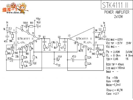
The STK4111 application circuit is shown as above.
(View)
View full Circuit Diagram | Comments | Reading(1205)
The STK4102 application circuit
Published:2011/6/20 10:31:00 Author:Seven | Keyword: application circuit
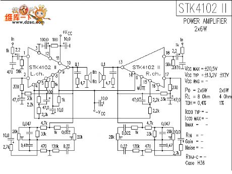
The STK4102 application circuit is shown in the figure:
(View)
View full Circuit Diagram | Comments | Reading(1185)
The video enhancing circuit
Published:2011/6/19 20:47:00 Author:qqtang | Keyword: video enhancing circuit
The video enhancing circuit is shown in the figure.
(View)
View full Circuit Diagram | Comments | Reading(667)
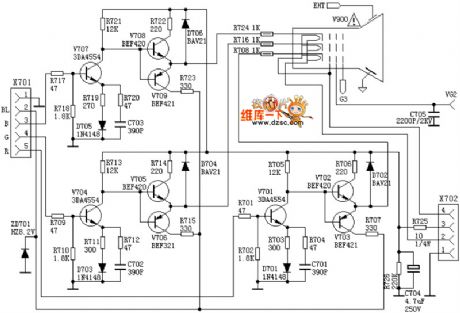
The TV video amplifier circuit
Published:2011/6/19 20:52:00 Author:qqtang | Keyword: video amplifier circuit
The TV video amplifier circuit is shown in the figure.
(View)
View full Circuit Diagram | Comments | Reading(673)
The TV video amplifier circuit (1)
Published:2011/6/19 20:51:00 Author:qqtang | Keyword: video amplifier
The TV video amplifier circuit (1) is shown in the figure.
(View)
View full Circuit Diagram | Comments | Reading(666)
The audio inductance wireless headphone circuit
Published:2011/6/19 21:39:00 Author:qqtang | Keyword: audio inductance, wireless headphone
The audio inductance wireless headphone circuit is shown in the figure.
(View)
View full Circuit Diagram | Comments | Reading(794)
The 6l6 single terminal headphone amplifier circuit
Published:2011/6/19 21:40:00 Author:qqtang | Keyword: single terminal, headphone amplifier
The 6l6 single terminal headphone amplifier circuit is shown in the figure.
(View)
View full Circuit Diagram | Comments | Reading(4681)
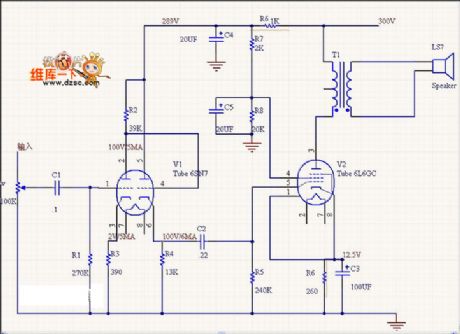
The TC1 vacuum pipe headphone power amplifier circuit
Published:2011/6/19 21:44:00 Author:qqtang | Keyword: vacuum pipe, headphone, power amplifier
The TC1 vacuum pipe headphone power amplifier circuit is shown in the figure.
(View)
View full Circuit Diagram | Comments | Reading(870)
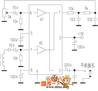
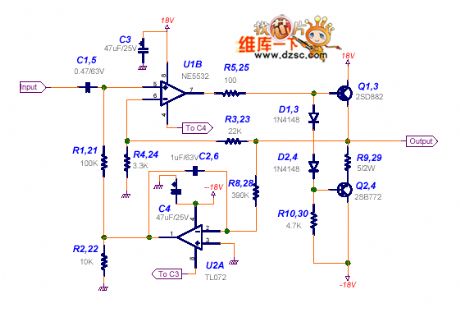
The headphone amplifier circuit composed of the dual op-amp (OPA2604, et al)
Published:2011/6/19 21:53:00 Author:qqtang | Keyword: headphone amplifier, dual op-amp
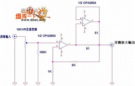
The headphone amplifier circuit composed of the dual op-amp (OPA2604, et al) is shown in the figure.
(View)
View full Circuit Diagram | Comments | Reading(2538)
The ZEN headphone amplifier circuit
Published:2011/6/19 21:50:00 Author:qqtang | Keyword: headphone, amplifier circuit
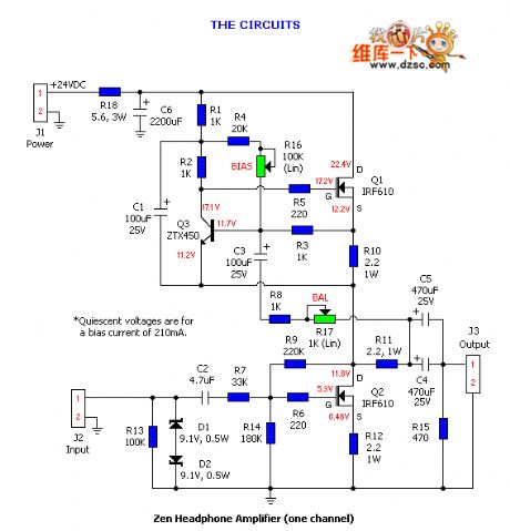
The ZEN headphone amplifier circuit is shown in the figure.
(View)
View full Circuit Diagram | Comments | Reading(1091)
The low-voltage 60min timing circuit
Published:2011/6/19 22:41:00 Author:qqtang | Keyword: low-voltage, timing circuit
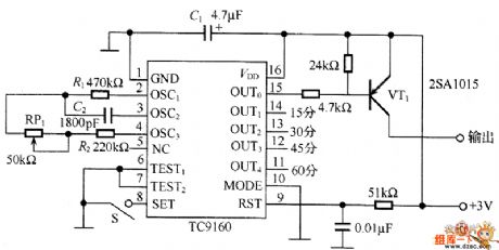
In the circuit, TC9l60 is the timer integrated circuit, in the chip there is an oscillating circuit and 20-bit binary counter, the maximum timing is 60min, the oscillating frequency is 1KHz. The timer resistance RT is higher than 20OkΩ. According to C2≤1/(2.2fcRt), if C2 is 1800pF, then Rt=216.76kΩ, which is serially connected with R2. The output is the leakage pole open type, OUT1~4 is graded every 15min, and it stops when the timing is over, by this moment, the power consumption is only 1μA.
(View)
View full Circuit Diagram | Comments | Reading(565)
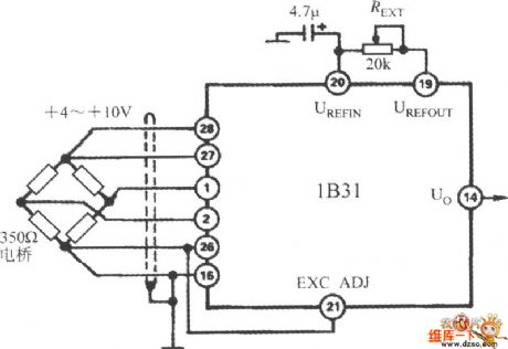
The The wide band reacting adjuster 1B31 circuit of motivated voltage rising
Published:2011/6/19 22:31:00 Author:qqtang | Keyword: wide band, reacting adjuster, motivated voltage
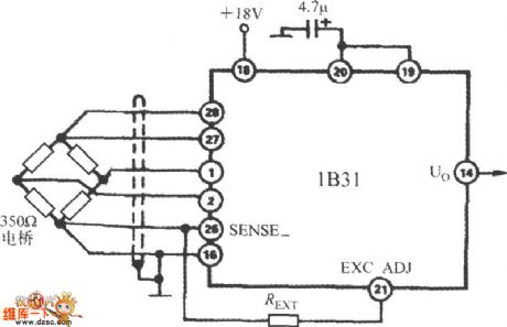


When the 19-pin of wide band reacting adjuster 1B31 touches the 20-pin, the programmable electric bridge motivation source outputs a voltage of UEXC=+10V. To rise UEXC to +10~+15V, we must fix a resistor REXT between EXC ADJ and SENSE, the circuit is shown in the figure. The REXT value is decided by the following formula (the unit of the resistance is kΩ):
of which: (View)
View full Circuit Diagram | Comments | Reading(574)
The (wide band reacting adjuster 1B31) circuit of motivated voltage lessening
Published:2011/6/19 22:23:00 Author:qqtang | Keyword: wide band, reacting adjuster, motivated voltage
View full Circuit Diagram | Comments | Reading(513)
The U6046B timer application circuit
Published:2011/6/19 22:17:00 Author:qqtang | Keyword: timer, application circuit
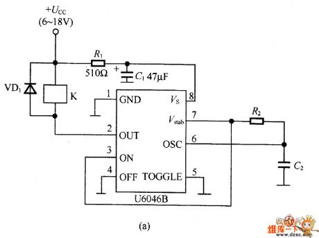
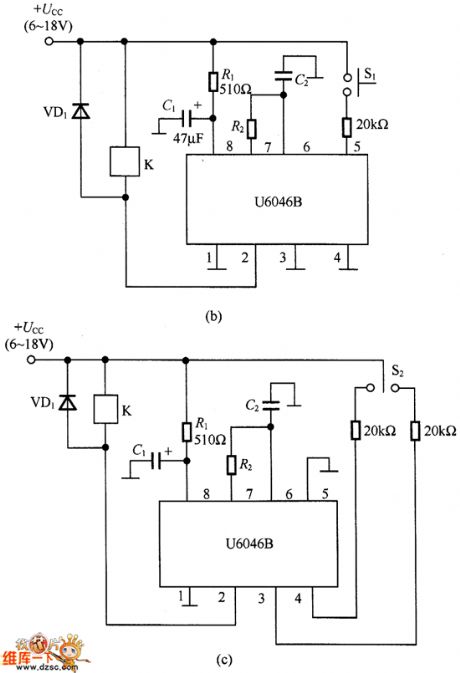
In figure 5-22 is the U6046B timer application circuit. U6046B is the long-time limiting timer integrated chip, which is in 8-pin DIP package, the timing span is from 3.7s to 20h, the power supply voltage is from 6~18v. In figure 5-22 (a) is the single stable timing circuit composed of U6046B, the working voltage +Ucc is added on 8-pin after being limited by R1 and filtered by C1, then there generates a 5.2V stable ouput voltage on 7-pin of U6046B and the voltage is the input of 3-pin, so that U6046B is started. The sucker current on 2-pin makes the relay K close, the timing td is started.
(View)
View full Circuit Diagram | Comments | Reading(1611)
The LC-KING A headphone amplifier circuit
Published:2011/6/19 22:06:00 Author:qqtang | Keyword: headphone amplifier
The LC-KING A headphone amplifier circuit is shown in the figure.
(View)
View full Circuit Diagram | Comments | Reading(809)
The AB type amplifier circuit of LC-KING
Published:2011/6/19 22:05:00 Author:qqtang | Keyword: amplifier circuit
The AB type amplifier circuit of LC-KING is shown in the figure.
(View)
View full Circuit Diagram | Comments | Reading(713)
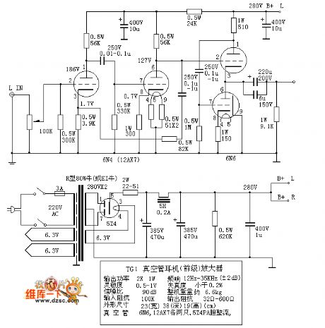
12AX7--the Shigeto tube pre-amplifier circuit
Published:2011/6/19 1:14:00 Author:Seven | Keyword: Shigeto, pre-amplifier circuit
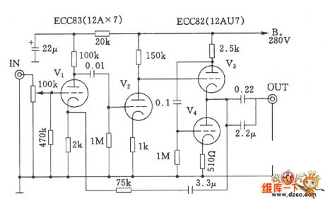
12AX7--the Shigeto tube pre-amplifier circuit is shown in the figure.
(View)
View full Circuit Diagram | Comments | Reading(4421)
The 100W op-amp circuit
Published:2011/6/19 2:34:00 Author:Seven | Keyword: op-amp circuit
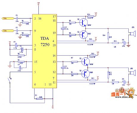
The 100W op-amp circuit is shown in the figure.
(View)
View full Circuit Diagram | Comments | Reading(1401)
Integrated Voltage Comparator Circuit
Published:2011/6/14 23:17:00 Author:Robert | Keyword: Integrated, Voltage, Comparator
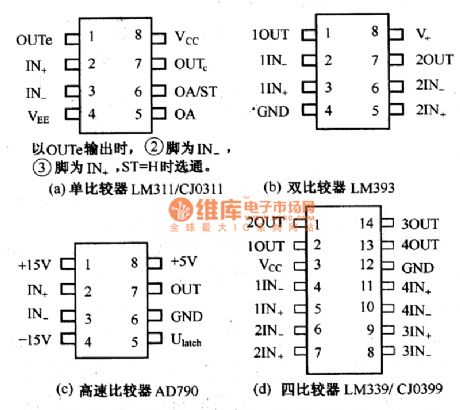
The integrated voltage comparator is a special operational amplifier. The operational amplifier is working in open-loop mode. Because its open-loop gain is bery big, the comparator's output is offen high voltage level or low voltage level.
The integrated voltage comparator is a common signal processing unit circuit which is widely used in compare of signal amplitude and choice of signal amplitude and waveform transformation and shaping and so on.
Some common integrated voltage comparator's pinout is shown in the picture.
(a)Single Comparator LM311/CJ0311. (b)Double Comparator LM393. (c)High-Speed Comparator AD790. (d)Quatuor Comparator LM339/CJ-399.
(View)
View full Circuit Diagram | Comments | Reading(718)
Keyboard input circuit
Published:2011/6/17 11:38:00 Author:John | Keyword: Keyboard
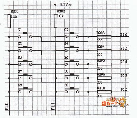
Keyboard circuit is mainly used to input data in order to achieve human-computer interaction. The design of system's keyboard is the realization of matrix keyboard through scanning. Keyboard circuit is as shown in the figure.
It can be seen from the figure that this matrix keyboard is composed of lines and columns. P1.0 and P1.1 compose columns of the keyboard and P1.2, P1.3, P1.4, P1.5 and P1.6 compose lines of the keyboard. Lines of the keyboard is regarded as a keyboard’s controling output end and columns of the keyboard is regarded as a keyboard’s controling input end.
(View)
View full Circuit Diagram | Comments | Reading(1588)
| Pages:197/250 At 20181182183184185186187188189190191192193194195196197198199200Under 20 |
Circuit Categories
power supply circuit
Amplifier Circuit
Basic Circuit
LED and Light Circuit
Sensor Circuit
Signal Processing
Electrical Equipment Circuit
Control Circuit
Remote Control Circuit
A/D-D/A Converter Circuit
Audio Circuit
Measuring and Test Circuit
Communication Circuit
Computer-Related Circuit
555 Circuit
Automotive Circuit
Repairing Circuit