
Amplifier Circuit
Index 194
The EF86+6SN7+6L6 push-pull circuit
Published:2011/6/20 21:59:00 Author:Seven | Keyword: push-pull circuit
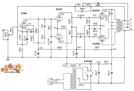
The EF86+6SN7+6L6 push-pull circuit is shown in the figure.
(View)
View full Circuit Diagram | Comments | Reading(14343)
The 6SN7+300B single terminal circuit
Published:2011/6/20 22:01:00 Author:Seven | Keyword: single terminal circuit
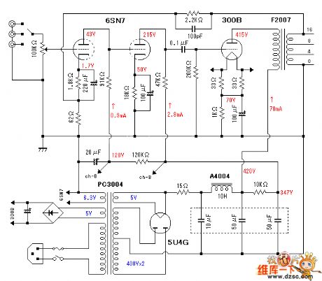
The 6SN7+300B single terminal circuit is shown in the figure.
(View)
View full Circuit Diagram | Comments | Reading(7243)
The electronic valve difference common-gate phase-reversing circuit
Published:2011/6/20 22:01:00 Author:Seven | Keyword: electronic valve, common-gate

The electronic valve difference common-gate phase-reversing circuit is shown in theabove figure.
(View)
View full Circuit Diagram | Comments | Reading(976)
The IM3886 op-amp circuit
Published:2011/6/20 22:02:00 Author:Seven | Keyword: op-amp
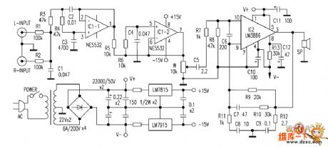
The IM3886 op-amp circuit is shown in the above circuit.
(View)
View full Circuit Diagram | Comments | Reading(930)
The isolation detection circuit
Published:2011/6/19 8:04:00 Author:Seven | Keyword: isolation detection
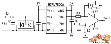
The simulation signal detection circuit is to convert the strong signal into the weak digital signals that dsp can read, and it must be sure of the isolation of the strong and weak electricity. The writer chooses the HP hcp17800a photoelectric coupler, whose linearity is 0.004%, and the impedance is 15kv/lμs when the common voltage is 1000v, the gain drift is 0.000 25v/℃, the band width is 100KHz. The concrete isolation detection circuit is shown in the figure.
(View)
View full Circuit Diagram | Comments | Reading(1014)
TGBT drive circuit
Published:2011/6/19 8:17:00 Author:Seven | Keyword: drive circuit
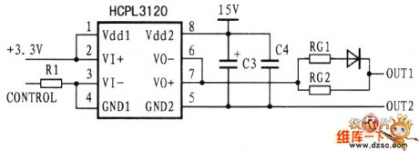
The pwm signal generated by dsp control circuit first crosses the drive circuit, and then controls the ON/OFF state of the igbt switch pipe. The writer chooses HP hcpl3120 specialized igbt drive circuit, see as the figure. The output and input of the drive circuit are isolated to each other, the drive circuit also has the function of LEV switching, it can convert the dsp +5 control voltage in the +15V igbt drive circuit, the drive circuit is equipped with the MORNSUN b0515 isolating power supply module.
(View)
View full Circuit Diagram | Comments | Reading(1863)
The PCL86 cow output amp circuit
Published:2011/6/21 9:57:00 Author:Borg | Keyword: output amp
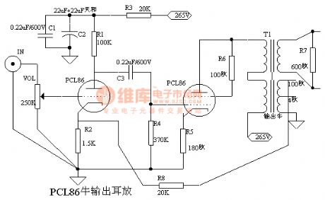
View full Circuit Diagram | Comments | Reading(4680)
The single channel amplifier circuit
Published:2011/6/22 1:11:00 Author:Borg | Keyword: single channel, amplifier
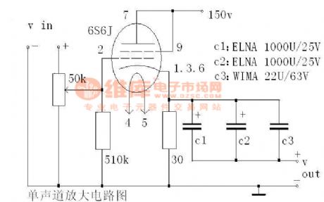
The single channel amplifier circuit (View)
View full Circuit Diagram | Comments | Reading(677)
The OCL stereo sound power amplifier circuit
Published:2011/6/21 21:34:00 Author:qqtang | Keyword: stereo sound, power amplifier
The OCL stereo sound power amplifier circuit is shown as above.
(View)
View full Circuit Diagram | Comments | Reading(1873)
The block frequency reducing circuit of capacitors (wide band reaction signal regulator 1B31)
Published:2011/6/23 1:06:00 Author:qqtang | Keyword: block frequency, wide band

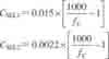
By the external capacitors CSEL1 and CSEL2, the block frequency of the low-pass filter can be set under 1KHz, which can meet the narrow band need, see as the figure. The capacitance computing formula is as follows.
(View)
View full Circuit Diagram | Comments | Reading(649)
The block frequency rising (wide band reaction signal regulator 1B31) circuit with resistors
Published:2011/6/23 11:24:00 Author:qqtang | Keyword: block frequency, signal regulator, resistor
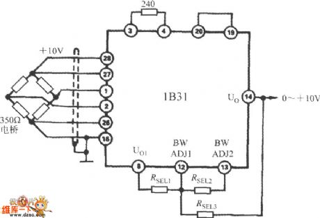
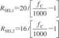
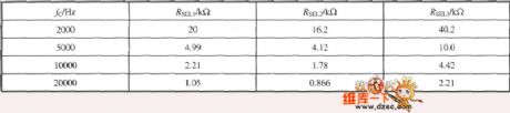
By 3 external resistors, the block frequency can be risen from 1KHz to 20KHz, which can meet the need of wide band. The circuit is shown in the figure. The resistance value computing formulais as follows:
In the formula, the unit of RSEL1~RSEL3 is kΩ. Besides, the resistance valuecan be chosen according to the table.
(View)
View full Circuit Diagram | Comments | Reading(739)
The STK4181 application circuit
Published:2011/6/19 9:43:00 Author:Seven | Keyword: application circuit
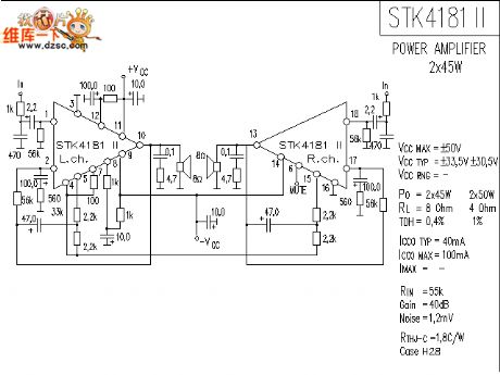
The STK4181 application circuit is shown in the figure.
(View)
View full Circuit Diagram | Comments | Reading(2574)
the STK4172 application circuit
Published:2011/6/20 22:04:00 Author:Seven | Keyword: application circuit

The STK4172 application circuit is shown in the above figure.
(View)
View full Circuit Diagram | Comments | Reading(5824)
adjustable non-steady-state circuit
Published:2011/6/21 0:50:00 Author:John
Adjustable non-steady-state circuit is shown.
(View)
View full Circuit Diagram | Comments | Reading(566)
Non-steady-state circuit with adjustable pulse width
Published:2011/6/21 0:50:00 Author:John | Keyword: adjustable pulse width
Non-steady-state circuit with adjustable pulse width is shown.
(View)
View full Circuit Diagram | Comments | Reading(529)
The STK4162 application circuit
Published:2011/6/20 22:05:00 Author:Seven | Keyword: application circuit

The STK4162 application circuit is shown in theabove figure.
(View)
View full Circuit Diagram | Comments | Reading(4404)
The STK4132 application circuit
Published:2011/6/20 0:57:00 Author:Seven | Keyword: application circuit
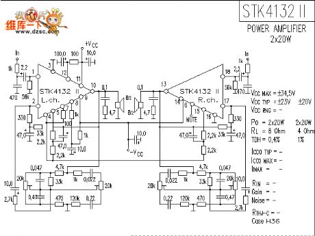
The STK4132 application circuit is shown in the figure.
(View)
View full Circuit Diagram | Comments | Reading(5705)
The long-term timing circuit composed of 555
Published:2011/6/23 11:15:00 Author:qqtang | Keyword: long-term, timing circuit
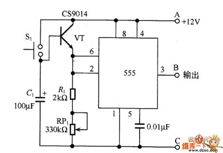
In the figure is the long-term timing circuit composed of 555. When S1 is pressed, timing is starting, and the time can be changed by adjusting RP1, the timing range is 3~220min. If capacitor C1 is 2200μF, then the timing range is 40~48h. The 3-pin of 555 outputs the timing control signal. If the circuit is used to control large power controller, a relay can be fixed between B and C or A and B, the touch spot of the relay is to control all kinds of timing loading.
(View)
View full Circuit Diagram | Comments | Reading(1084)
The 555 time delay energy-saving lamp circuit
Published:2011/6/23 10:59:00 Author:qqtang | Keyword: time delay, energy-saving lamp
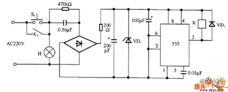
In the circuit is the 555 time delay energy-saving lamp circuit, which can be used at the stair exit and corridor. By pressing S1, the relay K is conducting, at the same time, the lamp K is glowing, the touch spot K1 is closed and locking the power supply. H is put out in 2min, after the light is off, the power consumption is very low, so the aim of saving power is fulfilled.
(View)
View full Circuit Diagram | Comments | Reading(1645)
The NE555 timing circuit of ±15v power supply
Published:2011/6/23 3:24:00 Author:qqtang | Keyword: timing circuit, power supply
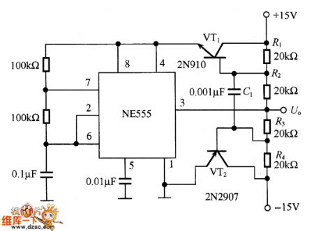
In the figure is the NE555 timing circuit of ±15v power supply. In the circuit, to get a dual-channel capability and work in double power supplies, we can add a floating different working voltage on the power supply terminal of NE555. The resistors R1~R4 and transistors (VT1 and VT2) compose a LEV moving net, which can generate the required floating voltage. The capacitor C1 is used to impede the high frequency oscillation generated by the impedance timer when it is jumping.
(View)
View full Circuit Diagram | Comments | Reading(2816)
| Pages:194/250 At 20181182183184185186187188189190191192193194195196197198199200Under 20 |
Circuit Categories
power supply circuit
Amplifier Circuit
Basic Circuit
LED and Light Circuit
Sensor Circuit
Signal Processing
Electrical Equipment Circuit
Control Circuit
Remote Control Circuit
A/D-D/A Converter Circuit
Audio Circuit
Measuring and Test Circuit
Communication Circuit
Computer-Related Circuit
555 Circuit
Automotive Circuit
Repairing Circuit